Every ASIC miner sitting on your shelf or heating your home started as a concept on an engineer’s workstation. Between that first line of RTL code and the moment your Antminer S21 hashes its first share, an extraordinarily precise chain of design, fabrication, testing, and packaging takes place — one that pushes the absolute limits of physics and engineering.
Understanding this process does more than satisfy curiosity. It makes you a better miner. When you know what sits inside that metal enclosure — the silicon, the interconnects, the billions of transistors switching at GHz frequencies — you can make smarter decisions about which hardware to buy, how to maintain it, and when to repair versus replace.
This is the deep-dive guide the Bitcoin mining community deserves. No fluff, no corporate filler. Just the raw, technical truth about how an ASIC goes from concept to completion — and why it matters for decentralizing Bitcoin’s hash rate.
What Is an ASIC and Why Does It Dominate Bitcoin Mining?
An Application-Specific Integrated Circuit (ASIC) is a chip designed from the ground up to do one thing — and do it with ruthless efficiency. Unlike CPUs or GPUs that juggle millions of different instruction types, a Bitcoin mining ASIC is hardwired to execute the SHA-256 hash function and nothing else. Every transistor, every logic gate, every metal interconnect is optimized for that single purpose.
The result? Orders of magnitude more performance per watt than any general-purpose processor. A modern mining ASIC like the BM1370 (used in the Antminer S21 Pro) achieves roughly 15 J/TH — meaning it produces one terahash per second of computational output for just 15 joules of energy. Compare that to GPU mining circa 2013, where you might burn 1,000+ J/TH. That is a 60x+ improvement in energy efficiency, and it is the reason ASICs completely displaced GPUs from Bitcoin mining.
The Three Classes of ASIC Design
Not all ASICs are created equal. The semiconductor industry recognizes three broad categories:
| Type | Description | Bitcoin Mining Relevance |
|---|---|---|
| Full Custom | Designed from scratch, transistor by transistor. Maximum optimization for performance, power, and area. | This is what Bitmain, MicroBT, and other mining chip designers use. Every BM-series and WhatsMiner chip is a full-custom design. |
| Semi-Custom | Uses pre-verified standard cells arranged into custom configurations. Faster time-to-market, lower NRE cost. | Some early-generation mining chips used semi-custom flows. Occasionally seen in open-source mining chip prototypes. |
| Platform / Structured | Pre-built platform with customizable logic blocks. Fastest to market, lowest cost, least optimized. | Not viable for competitive Bitcoin mining — efficiency gap is too large. |
For Bitcoin mining, full-custom is the only path that makes economic sense at scale. When fractions of a joule per terahash determine profitability, there is zero room for the compromises inherent in semi-custom or platform approaches.
Phase 1: Architecture and RTL Design
The ASIC fabrication journey begins not in a cleanroom, but at a workstation. Engineers define the chip’s architecture — how many SHA-256 cores, the clock tree topology, power delivery network, I/O interfaces, and on-chip voltage regulators.
Defining the SHA-256 Pipeline
A Bitcoin mining ASIC’s core computational unit is the SHA-256 engine. Each chip contains hundreds or thousands of these engines running in parallel. The design team decides critical parameters:
- Pipeline depth: How many clock cycles to complete one SHA-256 double-hash. Deeper pipelines allow higher clock frequencies but consume more area.
- Parallelism: How many independent hash engines run simultaneously. More cores = more hashrate, but also more power and heat.
- Clock frequency targets: Modern mining ASICs operate in the 400–800 MHz range, with some pushing higher through aggressive voltage scaling.
- Power delivery: On-chip voltage regulators, decoupling capacitor placement, and power grid density — all critical for supplying stable current to billions of switching transistors.
The architecture is captured in RTL (Register Transfer Level) code — typically Verilog or SystemVerilog. This is the “source code” of the chip. It describes every register, every logic gate, every multiplexer in a hardware description language that can be simulated and verified before a single atom of silicon is touched.
Electronic Design Automation (EDA)
Modern ASICs contain billions of transistors. No human can manually route that complexity. EDA tools from vendors like Synopsys, Cadence, and Siemens EDA handle the heavy lifting:
- Logic synthesis: Converts RTL into a gate-level netlist — the actual logic gates that will be fabricated.
- Place and route: Determines the physical location of every cell and the metal wires connecting them.
- Timing analysis: Verifies that signals arrive at their destinations within the clock period — critical for hitting frequency targets.
- Power analysis: Estimates dynamic and static power consumption across operating conditions.
- DRC/LVS: Design Rule Checks and Layout vs. Schematic verification ensure the physical layout is manufacturable and matches the intended circuit.
This phase can take 6–18 months depending on chip complexity. For a major mining ASIC iteration (like the jump from BM1366 to BM1370), expect the longer end of that range.
Phase 2: Fabrication — Turning Silicon Into Hashrate
Once the design is finalized, taped out, and photomasks are ordered, the physical fabrication begins at a semiconductor foundry — most likely TSMC or Samsung.
Wafer Preparation
Everything starts with ultrapure silicon. The Czochralski process grows a single-crystal silicon ingot by slowly pulling a seed crystal from a crucible of molten silicon at roughly 1,425 degrees Celsius. The resulting ingot — typically 300mm (12 inches) in diameter for modern processes — is sliced into wafers less than 1mm thick and polished to atomic-level smoothness.
Each 300mm wafer will yield hundreds of individual ASIC dies, depending on die size. A typical mining ASIC die might be 50–120 mm² depending on the process node and core count.
Photolithography: Printing Circuits With Light
Photolithography is the single most critical step in chip fabrication. It transfers the circuit patterns from photomasks onto the silicon wafer using ultraviolet light — or, for advanced nodes (5nm and below), extreme ultraviolet (EUV) lithography at 13.5nm wavelength.
The process repeats for each layer of the chip. A modern ASIC can have 50–80 individual layers, each requiring its own photomask alignment, exposure, and development cycle. The precision required is staggering: features are measured in nanometers, and overlay accuracy between layers must be within a few nanometers.
Etching, Deposition, and Doping
After each photolithography step, material is either added or removed:
- Etching: Reactive ion etching (RIE) or wet chemical etching removes material where the photoresist has been developed away, carving transistor gates, trenches, and vias into the silicon and dielectric layers.
- Deposition: Chemical vapor deposition (CVD), physical vapor deposition (PVD), and atomic layer deposition (ALD) add thin films of insulators, conductors, and semiconductors. Each layer might be just a few atoms thick.
- Ion implantation: Dopant atoms (boron for p-type, phosphorus or arsenic for n-type) are accelerated to high energies and fired into the silicon substrate, creating the semiconductor junctions that form transistors.
These steps repeat dozens of times, building the chip layer by layer from the transistor level up through the metal interconnect stack.
Metallization: The Wiring
Above the transistor layer sits the interconnect stack — typically 8–15 layers of copper wiring separated by low-k dielectric insulators. These metal layers carry signals and power throughout the chip. Lower metal layers are thinner and handle local connections between nearby transistors; upper metal layers are thicker and route power and global signals across the die.
The quality of this interconnect stack directly impacts the chip’s power efficiency. Resistance in the power delivery network (IR drop) wastes energy as heat — exactly what you do not want in a mining ASIC that already generates substantial thermal load.
Phase 3: Testing — Separating Good Dies From Bad
No fabrication process is perfect. Defects are inevitable. The testing phase determines which dies on a wafer actually work and how well they perform.
Wafer-Level Testing (Wafer Sort)
Before the wafer is diced into individual chips, each die is probed and tested in place. Automated test equipment (ATE) contacts tiny pads on the die surface through probe cards and runs functional test patterns. Dies that fail are marked with an ink dot and discarded after dicing.
Yield — the percentage of good dies per wafer — is a critical economic metric. For a mature process node, yields of 85–95% are common. For bleeding-edge nodes in early production, yields can drop below 50%, dramatically increasing the per-chip cost.
Speed Binning
Not all passing dies perform identically. Some hash faster. Some run cooler. Some tolerate higher voltages. Speed binning sorts chips into performance tiers based on measured characteristics. This is why you see efficiency differences between, say, an Antminer S21 and S21 Pro despite using the same BM1370 chip — the Pro models use top-bin chips that achieve better J/TH at higher hashrates.
| Bin Tier | Characteristics | Typical Miner Placement |
|---|---|---|
| Top Bin | Highest frequency, lowest leakage, best efficiency | Flagship models (e.g., S21 Hydro, S21 Pro) |
| Mid Bin | Good performance, acceptable efficiency | Standard models (e.g., S21, T21) |
| Low Bin | Lower frequency or higher leakage, still functional | Budget/value models, underclocked configs |
| Fail | Does not meet minimum specifications | Discarded or recycled |
Understanding speed binning is practical knowledge for any miner. When D-Central’s ASIC repair technicians diagnose a hashboard, they are looking at chip-level performance — identifying which chips on the board are underperforming or failing, and whether replacements are viable.
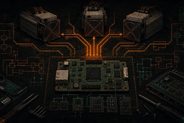
Phase 4: Packaging — From Bare Die to Hashboard-Ready Component
A bare silicon die is incredibly fragile. Packaging transforms it into a robust component that can be soldered onto a hashboard PCB, connected to power delivery circuits, and cooled by heatsinks and fans.
Modern Packaging Technologies for Mining ASICs
Mining ASICs predominantly use BGA (Ball Grid Array) or QFN (Quad Flat No-Lead) packages:
- BGA: Solder balls on the underside of the package connect directly to the PCB. Offers excellent thermal and electrical performance. Used on most modern mining hashboards.
- QFN: Exposed pad on the bottom provides a direct thermal path to the PCB. Smaller footprint than BGA. Common on compact mining designs and some open-source mining hardware like the Bitaxe.
- Flip-chip: The die is flipped upside down and bonded directly to the substrate, shortening interconnect paths and improving thermal dissipation. Increasingly used in high-performance mining chips.
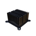
The package also includes decoupling capacitors, thermal interface materials, and sometimes integrated heat spreaders — all engineered to keep the chip running within its thermal envelope while delivering maximum hashrate.
Final Test and Reliability Screening
Packaged chips undergo a final battery of tests:
- Functional testing: Full operational verification at nominal voltage and frequency.
- Burn-in: Chips are operated at elevated temperature and voltage (typically 125 degrees Celsius, 10–15% overvoltage) for 24–168 hours. This accelerates infant mortality failures — chips that would die in the first weeks of operation fail during burn-in instead, so they never reach customers.
- System-level validation: Sample chips are tested on actual hashboard reference designs to verify real-world mining performance.
Only chips that survive every stage ship to hashboard manufacturers — where they are soldered alongside voltage regulators, clock generators, and communication interfaces to form the hashboards that slot into your miner.
From Fab to Your Mining Rig: The Supply Chain
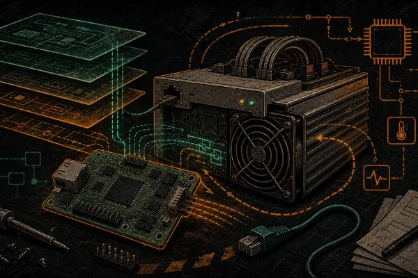
The path from packaged ASIC chip to a running miner on your shelf involves several more steps:
- Hashboard assembly: Chips are soldered onto PCBs alongside power delivery and communication circuitry. Each hashboard contains dozens to hundreds of ASIC chips.
- Miner assembly: Hashboards are installed in an enclosure with control boards, fans, power connectors, and firmware.
- QC and stress test: Completed miners run for 24–72 hours under load to verify hashrate, power consumption, and thermal stability.
- Distribution: Miners ship to distributors and resellers worldwide — including companies like D-Central Technologies that provide the full lifecycle: sourcing, configuration, hosting, repair, and ongoing support.
Why ASIC Fabrication Knowledge Matters for Home Miners
You might wonder why a home miner needs to care about photolithography and dopant implantation. Here is why this knowledge is power:
Smarter Hardware Purchases
When a manufacturer announces a “5nm” or “3nm” mining chip, you now understand what that actually means — smaller transistors, lower power per hash, more cores per die. You can evaluate whether a generational jump justifies the price premium, or whether an older-generation miner running as a space heater delivers better ROI for your specific situation.
Better Repair Decisions
ASIC chips can fail for reasons rooted in their fabrication: electromigration in copper interconnects, thermal cycling stress on solder joints, dopant migration over time. Understanding these failure modes helps you make informed decisions when a hashboard goes down. Is a chip-level repair worth it? Should you replace the full board? D-Central’s repair team deals with these questions every day across 38+ ASIC models.
Appreciating the Decentralization Challenge
ASIC fabrication requires multi-billion-dollar foundries, years of R&D, and deep supply chain relationships. This concentration of capability in a few companies (TSMC, Samsung, Intel Foundry) represents a centralization risk for Bitcoin. Supporting open-source mining initiatives — like the Bitaxe, NerdAxe, and other open-hardware projects — is one way the community fights back against this concentration. D-Central has been a pioneer in this space since the earliest Bitaxe days, manufacturing the original Bitaxe Mesh Stand and developing heatsinks, cases, and accessories for the open-source mining ecosystem.
The Process Node Arms Race: Where Mining ASICs Are Headed
The Bitcoin mining industry is locked in a perpetual arms race for better efficiency. Each new process node — from 28nm to 16nm to 7nm to 5nm to 3nm — delivers roughly 25–40% improvement in energy efficiency per hash.
| Process Node | Example Mining Chip | Approx. Efficiency (J/TH) | Era |
|---|---|---|---|
| 28nm | BM1385 (Antminer S7) | ~250 J/TH | 2015–2016 |
| 16nm | BM1387 (Antminer S9) | ~98 J/TH | 2016–2019 |
| 7nm | BM1397 (Antminer S17) | ~40 J/TH | 2019–2021 |
| 5nm | BM1366 (Antminer S19 XP) | ~21.5 J/TH | 2022–2024 |
| 5nm (advanced) | BM1370 (Antminer S21) | ~15 J/TH | 2024–2026 |
| 3nm | Next-gen (announced/rumored) | ~10–12 J/TH (projected) | 2026+ |
But there is a catch. Each new node costs exponentially more to develop and fabricate. A single 3nm photomask set can exceed $30 million. Full chip development from RTL to production can run $500 million or more. This is why only a handful of companies can afford to play at the leading edge — and why every generation of mining hardware carries those costs embedded in its price tag.
The practical takeaway: do not blindly chase the newest generation. A well-maintained S19 or S21 at the right electricity rate still prints sats profitably. The “best” miner is always relative to your power cost, ambient temperature, and use case. A Bitcoin space heater running an older-gen chip in a Canadian winter is extracting value that pure efficiency numbers do not capture.
Frequently Asked Questions
What does “ASIC” stand for, and why are ASICs used in Bitcoin mining?
ASIC stands for Application-Specific Integrated Circuit. Unlike CPUs or GPUs that handle many tasks, a Bitcoin mining ASIC is designed exclusively to compute SHA-256 hashes. This specialization makes ASICs orders of magnitude more efficient than general-purpose hardware for mining — delivering vastly more hashrate per watt of electricity consumed.
What process node do current Bitcoin mining ASICs use in 2026?
As of 2026, the most efficient production mining ASICs use advanced 5nm process technology (e.g., Bitmain’s BM1370 in the Antminer S21 series). Next-generation 3nm mining chips have been announced or rumored from multiple manufacturers, with projected efficiency improvements to the 10–12 J/TH range.
What is speed binning, and how does it affect which miner I should buy?
Speed binning is the process of sorting manufactured chips by performance. Top-bin chips run at higher frequencies with lower power consumption — these go into premium models. Lower-bin chips are still functional but less efficient, ending up in standard or budget models. The same chip design can produce meaningfully different mining performance depending on which bin it falls into.
Why do ASIC miners fail, and can they be repaired?
Common failure modes trace back to fabrication-level phenomena: electromigration (copper atoms moving in interconnects under sustained current), thermal cycling stress (repeated heating and cooling cracking solder joints), and voltage stress damaging gate oxides. Many of these failures are repairable at the chip level by skilled technicians. D-Central Technologies operates one of Canada’s largest ASIC repair facilities, servicing 38+ miner models with chip-level diagnostics and board repair.
How does ASIC fabrication relate to mining decentralization?
ASIC fabrication is concentrated in a few foundries (primarily TSMC), and chip design is dominated by a small number of companies. This creates supply chain centralization that can affect miner availability and pricing. Open-source mining hardware projects like Bitaxe and NerdAxe aim to diversify the ecosystem by making chip designs and board schematics publicly available, allowing smaller manufacturers to participate. D-Central has been a pioneer in supporting this movement since the earliest days of the Bitaxe project.
Is it worth buying a miner with an older process node chip?
Absolutely — depending on your use case. Older-generation miners (like the S9 on 16nm or S17 on 7nm) have lower upfront costs and can still be profitable at low electricity rates. They also excel as Bitcoin space heaters, where the “waste” heat displaces conventional heating costs. The best miner for you depends on your electricity price, climate, noise tolerance, and whether you value the heating benefit.
What is the difference between a mining ASIC chip and a full miner unit?
The ASIC chip is the raw silicon die — the computing engine that performs SHA-256 hashes. A full miner unit contains multiple hashboards (each populated with dozens to hundreds of ASIC chips), a control board running firmware, power supply connections, cooling fans, and an enclosure. The chip is one component in a complete system. When a miner fails, the root cause is often a single chip or a small cluster of chips on one hashboard — which is why chip-level repair is both possible and economical.
Where can I get my mining ASIC repaired in Canada?
D-Central Technologies operates out of Laval, Quebec, and is Canada’s leading Bitcoin mining hardware service provider. With chip-level diagnostic equipment and experience across 38+ ASIC models from Bitmain, MicroBT, Innosilicon, Canaan, and others, D-Central provides professional hashboard repair, component replacement, and performance optimization. Visit the ASIC Repair page for details.