
Creating a Home Mining Farm: Scaling Up from a Single ASIC
Welcome to the world of home cryptocurrency mining! In this comprehensive guide, we’ll explore how to create and scale a
4479 Desserte Nord Autoroute 440, Laval, QC H7P 6E2
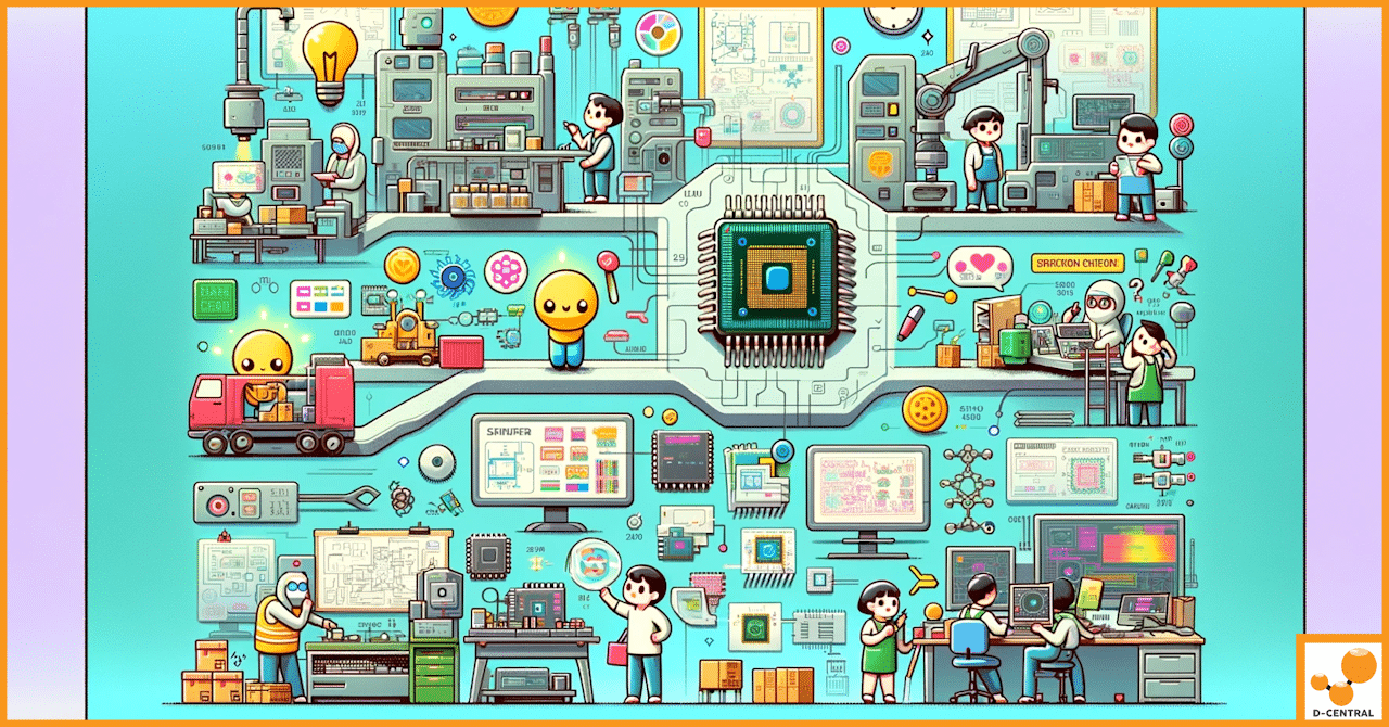
In the ever-evolving landscape of digital technology and cryptocurrency, Application-Specific Integrated Circuits (ASICs) stand out as pivotal components that drive innovation and efficiency. ASICs, by design, are engineered to perform specific tasks with unparalleled precision and speed, distinguishing them from general-purpose processors. This specialization allows ASICs to deliver optimal performance for targeted applications, making them indispensable in a wide array of technological domains, from consumer electronics to complex data processing systems.
The significance of ASICs is particularly pronounced in the realm of Bitcoin mining, a competitive and resource-intensive process that underpins the Bitcoin network. Here, ASICs play a crucial role by offering the computational horsepower necessary to solve complex cryptographic puzzles, a fundamental aspect of maintaining and securing the blockchain. The advent of ASIC technology in Bitcoin mining marked a paradigm shift, propelling the mining process to unprecedented levels of efficiency and productivity. This transition underscored the transformative potential of ASICs, not just in cryptocurrency mining but in shaping the future of digital transactions and blockchain technology.
At the forefront of this technological revolution is D-Central Technologies, a trailblazer in the Bitcoin mining landscape. Renowned for its expertise and innovation, D-Central Technologies has established itself as a leader in providing cutting-edge ASIC solutions. With a deep understanding of the intricacies of ASIC design and fabrication, D-Central Technologies offers a comprehensive suite of services that cater to the diverse needs of the Bitcoin mining community. From consultation and hardware sourcing to hosting operations and ASIC repairs, D-Central Technologies stands as a beacon of excellence, driving the advancement of Bitcoin mining and reinforcing the infrastructure of the digital economy.
Application-Specific Integrated Circuits (ASICs) are specialized microchips designed for a particular application or function, rather than intended for general-purpose use. Unlike standard microprocessors that can run a wide range of programs, ASICs are hardwired to perform specific tasks with optimal efficiency. This specialization enables ASICs to achieve higher performance, greater speed, and more energy-efficient operation for their designated tasks compared to general-purpose processors.
The importance of ASICs in electronics and computing cannot be overstated. They are integral to a multitude of devices and systems, enabling advancements in technology that require high-speed data processing, low power consumption, and compact form factors. From smartphones and consumer electronics to networking equipment and data centers, ASICs provide the necessary computational power and efficiency. In the realm of Bitcoin mining, ASICs have revolutionized the industry by offering unparalleled processing capabilities, significantly outperforming previous generations of mining hardware and contributing to the network’s security and efficiency.
ASICs can be categorized based on their design flexibility and the level of customization they offer. The three main types of ASICs are:
Each type of ASIC offers a unique set of advantages and trade-offs, allowing engineers and designers to choose the most appropriate technology based on the specific requirements of their application, including performance, power, area, and cost considerations.
The journey of creating an ASIC begins with the conceptualization phase, where the foundational idea is formed, and the need for a specialized circuit is identified. This stage involves a thorough analysis of the intended application to determine how an ASIC can provide a solution that off-the-shelf components cannot. Key considerations during this phase include:
This phase sets the stage for the entire project, laying down the primary objectives and constraints that will guide the design process.
Once the need for an ASIC is established, the next step involves defining the system requirements and specifications in detail. This stage translates the conceptual goals into technical parameters that will drive the design process. Specifications cover a wide range of aspects, including but not limited to:
Defining these specifications and constraints with precision is crucial, as they directly influence the feasibility and success of the ASIC in its intended application.
The complexity of modern ASICs necessitates the use of sophisticated software tools to aid in their design. Electronic Design Automation (EDA) tools are specialized software suites that provide a comprehensive environment for designing, analyzing, and verifying electronic systems. EDA tools play a pivotal role in the ASIC design phase by offering functionalities such as:
The use of EDA tools not only accelerates the design process but also enhances the accuracy and reliability of the final ASIC by identifying potential issues early in the development cycle.
The creation of a block diagram is a critical step in the preliminary design phase of an ASIC. A block diagram provides a high-level view of the ASIC’s architecture, illustrating the major components and their interconnections. This visual representation serves several important purposes:
The block diagram acts as a blueprint for the ASIC, guiding the detailed design and implementation stages that follow. It ensures that all team members have a clear understanding of the ASIC’s structure and functionality, promoting efficiency and coherence throughout the design process.
The foundation of the ASIC fabrication process begins with the selection and preparation of materials, predominantly silicon, due to its excellent semiconductor properties. Silicon wafers, the substrate for ASICs, are produced using the Czochralski process. This method involves melting highly pure silicon in a crucible and introducing a seed crystal at the surface. The seed crystal is then slowly withdrawn, pulling a cylindrical ingot of single-crystal silicon with it. The ingot is then sliced into thin wafers, polished to create a smooth, flawless surface essential for the subsequent fabrication steps.
Photomasks play a crucial role in the ASIC fabrication process, acting as stencils that transfer the ASIC design onto the silicon wafer. A photomask is created by coating a transparent substrate, typically glass, with a layer of light-blocking material and then using a high-precision laser or electron beam to etch the design onto the mask. Each layer of the ASIC design requires a separate photomask, and the accuracy and quality of these masks are critical for the fidelity of the final ASIC.
Photolithography is the process used to transfer the ASIC design from the photomask onto the silicon wafer. The wafer is first coated with a light-sensitive chemical called photoresist. The photomask is then aligned over the wafer, and ultraviolet light is shone through it. Where the light hits the photoresist, it changes its properties, allowing the exposed areas to be selectively removed. This leaves behind a pattern on the wafer that mirrors the design on the photomask, ready for the next step in the fabrication process.
Etching is used to remove material from the silicon wafer, creating the physical structures of the ASIC. There are several etching techniques, but the most common is reactive ion etching, which uses chemically reactive plasma to remove the unprotected areas of the wafer. After etching, the process of layering begins, where various materials are deposited onto the wafer to form the different layers of the ASIC, including insulating, conducting, and semiconducting layers. These steps are repeated multiple times, building up the ASIC layer by layer.
Dopant implantation is a critical step in the fabrication process that introduces impurities, or dopants, into the silicon wafer to modify its electrical properties. By carefully controlling the type and concentration of dopants, regions of the silicon can be made into n-type or p-type semiconductors, essential for forming the transistors that are the building blocks of the ASIC. This process is typically achieved through ion implantation, where dopant ions are accelerated and directed into the silicon substrate.
The final steps in the ASIC fabrication process involve metallization and the formation of interconnects. Metallization is the process of depositing metal layers onto the wafer to create electrical pathways between the various components of the ASIC. Aluminum or copper is commonly used for this purpose. These metal layers are then patterned and etched to form the intricate network of interconnects that enable communication and power distribution throughout the ASIC. The precision and integrity of these interconnects are vital for the overall performance and reliability of the final product.
Ensuring the reliability and performance of ASICs involves rigorous testing at various stages of the design and fabrication process. This testing is broadly categorized into pre-silicon validation and post-silicon validation, each employing specific techniques and methodologies to identify and rectify potential issues.
Pre-silicon validation is a critical phase in the ASIC development process, where the design is extensively tested before fabrication. This stage aims to verify the functionality and performance of the ASIC design against the specified requirements, using various simulation and verification techniques:
Once the ASIC is fabricated, it undergoes post-silicon validation to ensure that the physical chip meets the design specifications and performs as expected in real-world applications. This phase involves a series of tests:
Through these comprehensive pre-silicon and post-silicon validation processes, ASIC designers and manufacturers can ensure that the final product meets the highest standards of quality, performance, and reliability, fulfilling the stringent requirements of its intended applications.
After the ASIC fabrication and initial testing phases are completed, the focus shifts to packaging the silicon die and preparing the final product for delivery. This stage is crucial as the choice of packaging can significantly influence the ASIC’s performance, reliability, and its integration into the end application.
The packaging of an ASIC involves encasing the silicon die in a protective housing that facilitates electrical connections to the external environment while also providing mechanical support, heat dissipation, and protection from physical and environmental damage. Several packaging technologies are available, each with its own set of advantages and considerations:
The choice of packaging is influenced by factors such as the ASIC’s application, performance requirements, thermal management needs, and cost constraints. Effective packaging not only protects the die but also plays a critical role in heat dissipation, electrical performance, and the overall reliability of the ASIC.
Before the packaged ASICs are delivered to customers, they undergo a final round of testing and quality checks to ensure they meet all specifications and quality standards. This phase includes:
Upon successful completion of these final testing and quality assurance processes, the ASICs are deemed ready for delivery. They are then packaged and shipped to customers, accompanied by detailed documentation including test reports, handling instructions, and any necessary certifications, ensuring that the end-users receive fully functional, high-quality components ready for deployment in their applications.
The journey from conceptualizing an Application-Specific Integrated Circuit (ASIC) to its final delivery encapsulates a meticulous and sophisticated process that underscores the marvel of modern semiconductor technology. The ASIC fabrication process, with its intricate steps of design, material selection, photolithography, etching, doping, and packaging, exemplifies the pinnacle of engineering precision and innovation. Each phase, from the initial design conceptualization to the final quality checks, is imbued with a commitment to excellence, ensuring that the resulting ASICs meet the highest standards of performance, efficiency, and reliability.
ASICs have become indispensable in the fabric of contemporary technology, powering a myriad of devices and systems that form the backbone of our digital world. From consumer electronics to data centers, and notably in the realm of Bitcoin mining, ASICs deliver unparalleled computational power and efficiency, driving advancements and enabling new possibilities across industries.
As we stand on the cusp of new technological frontiers, the role of ASICs is set to become even more pivotal. The continuous push for higher performance, lower power consumption, and greater miniaturization demands the expertise and innovation that specialized companies like D-Central Technologies bring to the table. With its rich heritage in the Bitcoin mining landscape and a reputation for excellence in ASIC solutions, D-Central Technologies is uniquely positioned to meet the evolving needs of the industry.
We encourage those looking to harness the power of ASICs, whether for Bitcoin mining or other specialized applications, to explore the wealth of expertise and solutions offered by D-Central Technologies. With a commitment to quality, innovation, and customer satisfaction, D-Central stands ready to empower your technological endeavors, driving your projects to new heights of efficiency and success.
Discover how D-Central Technologies can elevate your operations with cutting-edge ASIC solutions by visiting D-Central Technologies. Join us in shaping the future of technology, one ASIC at a time.
What are Application-Specific Integrated Circuits (ASICs)?
ASICs are specialized microchips designed for a specific application or function, offering higher performance, greater speed, and more energy efficiency in their designated tasks compared to general-purpose processors.
Why are ASICs important in Bitcoin mining?
In Bitcoin mining, ASICs provide the essential computational power needed to solve complex cryptographic puzzles, significantly outperforming previous generations of mining hardware and enhancing the network’s security and efficiency.
What services does D-Central Technologies offer?
D-Central Technologies offers a comprehensive suite of services for the Bitcoin mining community, including consultation, hardware sourcing, hosting operations, and ASIC repairs, positioning itself as a leader in providing cutting-edge ASIC solutions.
What are the different types of ASICs?
ASICs can be categorized into Full Custom ASICs, designed from the ground up for high optimization; Semi-Custom ASICs, which use standard cells for a balance between customization and development cost; and Platform ASICs, offering a modular approach for quicker and less expensive market entry.
What is involved in the ASIC design phase?
The ASIC design phase involves conceptualization, where the need for a specialized circuit is identified, followed by definition of system requirements and use of Electronic Design Automation (EDA) tools for designing, analyzing, and verifying the ASIC.
How is an ASIC fabricated?
ASIC fabrication involves selecting and preparing materials like silicon, creating photomasks, transferring patterns onto the silicon wafer through photolithography, etching, layering, dopant implantation, metallization, and forming interconnects.
What testing and quality assurance processes do ASICs undergo?
ASICs undergo rigorous testing including pre-silicon validation (functional simulation, timing analysis, etc.), and post-silicon validation (functional testing, burn-in testing, etc.), as well as packaging and final quality checks before delivery.
How can D-Central Technologies aid in my Bitcoin mining or specialized application endeavors?
D-Central Technologies, with its expertise in ASIC solutions and services tailored to the Bitcoin mining industry, can provide the necessary resources, knowledge, and support to enhance your operations’ efficiency and success.
DISCLAIMER: D-Central Technologies and its associated content, including this blog, do not serve as financial advisors or official investment advisors. The insights and opinions shared here or by any guests featured in our content are provided purely for informational and educational purposes. Such communications should not be interpreted as financial, investment, legal, tax, or any form of specific advice. We are committed to advancing the knowledge and understanding of Bitcoin and its potential impact on society. However, we urge our community to proceed with caution and informed judgment in all related endeavors.
Related Posts
Welcome to the world of home cryptocurrency mining! In this comprehensive guide, we’ll explore how to create and scale a

Cryptocurrencies such as Bitcoin have the potential to revolutionize our financial systems, creating new opportunities for users and pushing us

Are you wondering if history is destined to repeat itself? The answer may lie in understanding aggregate price levels after