Every Bitcoin block mined in 2026 was secured by an Application-Specific Integrated Circuit — an ASIC. Not a CPU. Not a GPU. Not an FPGA. A chip designed from the transistor level up to do exactly one thing: compute SHA-256 hashes as fast and efficiently as silicon physics will allow. The entire security model of the Bitcoin network — now operating above 800 EH/s of global hashrate — rests on these purpose-built machines.
Understanding how ASIC chips go from concept to finished silicon is not just an academic exercise. For home miners, repair technicians, and anyone serious about Bitcoin’s decentralization, knowing what is inside your miner changes how you think about everything: hashrate efficiency, thermal management, why certain machines fail, and why the next generation is always a leap forward. This is the engineering that secures your money.
At D-Central Technologies, we have been repairing, modifying, and deploying ASICs since 2016. We have seen machines evolve from 16nm Antminer S9s to 5nm and 3nm beasts pushing hundreds of terahashes per second. We have diagnosed thousands of dead hashboards at the chip level. This guide is written from that hands-on experience — not from a semiconductor marketing brochure.
What Makes an ASIC an ASIC
An Application-Specific Integrated Circuit is a chip engineered to perform one defined task. In Bitcoin mining, that task is the SHA-256 double-hash computation used in the Proof-of-Work consensus mechanism. Every other component on a mining machine — the control board, fans, power supply, heat sinks — exists solely to support these chips in doing their single job.
The critical distinction from general-purpose processors:
- CPUs are designed to handle arbitrary instructions — they can run an operating system, a browser, a game. Flexibility is the point, and per-hash efficiency is terrible.
- GPUs parallelize thousands of simpler computations — better for hashing than CPUs, but still carrying massive overhead for graphics pipeline logic they never use in mining.
- FPGAs are reconfigurable logic arrays — they can be programmed for SHA-256, but the programmable routing fabric wastes silicon area and adds power overhead compared to a fixed design.
- ASICs hardwire the SHA-256 logic directly into silicon. No instruction decoder. No cache hierarchy. No programmable routing. Every transistor serves the hash function. This is why modern mining ASICs achieve 20-50+ joules per terahash (J/TH) efficiency — orders of magnitude better than any alternative.
Bitcoin mining’s transition from CPUs (2009) to GPUs (2010) to FPGAs (2011) to ASICs (2013) was not just a technology upgrade — it was an economic inevitability. SHA-256 is a fixed algorithm. A fixed algorithm demands a fixed-function chip. The only variable left to optimize is how small, how fast, and how power-efficient you can make that fixed function.
The ASIC Design Process: From Specification to Silicon
Designing a Bitcoin mining ASIC is a multi-year, multi-million-dollar effort that follows a rigorous semiconductor development flow. Here is what actually happens inside companies like Bitmain, MicroBT, and Intel (formerly running their Bonanza Mine project).
Step 1: Specification and Architecture
Everything starts with defining the target metrics. For a mining ASIC, the critical specifications are:
| Parameter | What It Means | Example Target (2026) |
|---|---|---|
| Hashrate per chip | SHA-256 hashes per second per die | 80-200+ GH/s |
| Energy efficiency | Joules per terahash (J/TH) | 15-21 J/TH |
| Process node | Semiconductor fabrication technology | 5nm / 3nm |
| Operating voltage | Core voltage range | 0.25-0.40V typical |
| Die size | Physical chip area in mm² | 40-120 mm² |
| Thermal design power | Heat output per chip in watts | 5-15W per chip |
The architectural phase determines how many SHA-256 cores fit on a single die, how the clock distribution network works, how power is delivered across the chip, and how temperature is managed. Every architectural decision is a tradeoff — more cores means more hashrate but also more power and heat. Lower voltage means better efficiency but tighter manufacturing tolerances and more sensitivity to process variation.
Step 2: RTL Design
The architecture is translated into Register Transfer Level (RTL) code, typically written in Verilog or SystemVerilog. RTL describes the chip’s behavior at the logic level — what happens on each clock cycle, how data flows between registers, how the SHA-256 rounds are pipelined or unrolled.
A SHA-256 hash computation involves 64 rounds of compression operations. ASIC designers have several strategies for implementing this:
- Fully unrolled pipeline: All 64 rounds are separate hardware stages. One hash completes every clock cycle after the pipeline fills. Maximum throughput, maximum silicon area.
- Partially unrolled: Groups of rounds share hardware with registers between stages. Balances area against throughput.
- Iterative: A single round engine loops 64 times per hash. Minimum area, lowest throughput per mm² of silicon.
Modern high-performance mining ASICs use fully or heavily unrolled designs because silicon area is cheap compared to the electricity cost savings from higher throughput per watt. The goal is to extract maximum hashes from every joule of energy consumed.
Step 3: Verification
Before spending millions on fabrication, the RTL design undergoes exhaustive verification. This includes:
- Functional simulation: Does the chip produce correct SHA-256 hashes for all possible inputs? Testbenches compare RTL output against known-good software implementations.
- Timing simulation: Can data propagate through all logic paths within the target clock period?
- Power analysis: What is the estimated power consumption at different activity levels and process corners?
- Corner case testing: Behavior at voltage extremes, temperature extremes, and worst-case process variation.
Verification typically consumes more engineering time than the design itself. A single undetected bug means an entire wafer run — millions of dollars — produces non-functional chips.
Step 4: Logic Synthesis and Physical Design
Logic synthesis transforms the RTL into a netlist of standard cells — the specific transistor-level building blocks available at the target process node. Electronic Design Automation (EDA) tools from companies like Synopsys and Cadence optimize this netlist for the designer’s priority: minimum area, maximum speed, or lowest power.
Physical design then places those cells on the die and routes the metal interconnects between them. This is where semiconductor physics gets real:
- Floorplanning: Positioning major functional blocks — SHA-256 cores, I/O pads, power grid connections, clock distribution trees.
- Placement: Arranging millions of individual standard cells to minimize wire length and signal delay.
- Clock tree synthesis: Building a balanced clock distribution network so every flip-flop in the chip receives the clock signal simultaneously (within picoseconds of skew).
- Routing: Connecting all cells with metal wires across multiple layers (modern processes use 10+ metal layers).
- Power grid design: Ensuring every cell receives stable supply voltage despite massive current draw. Mining ASICs run at ultra-low voltages (0.25-0.40V) with very high currents — power integrity is critical.
Step 5: Signoff and Tapeout
Before the design is sent to the foundry, it passes through a gauntlet of signoff checks:
- Design Rule Check (DRC): Does the layout comply with the foundry’s manufacturing constraints?
- Layout vs. Schematic (LVS): Does the physical layout match the intended circuit?
- Static Timing Analysis (STA): Do all signal paths meet timing at worst-case conditions?
- IR Drop Analysis: Is voltage delivered to every cell above minimum operating threshold?
- Electromigration Check: Will the metal wires survive years of continuous high-current operation?
Once all checks pass, the design is “taped out” — the final GDSII layout files are delivered to the semiconductor foundry (TSMC, Samsung, or similar). From tapeout to first silicon typically takes 2-4 months.
Manufacturing: From Wafer to Packaged Chip
Wafer Fabrication
The foundry prints the chip design onto silicon wafers using photolithography. At 5nm and 3nm nodes — the cutting edge used for the latest mining ASICs — this involves Extreme Ultraviolet (EUV) lithography, which uses 13.5nm wavelength light to pattern features smaller than a virus.
A single 300mm wafer can contain thousands of mining ASIC dies. The yield — the percentage of functional dies per wafer — is a closely guarded trade secret and a critical factor in chip economics. Early production runs on new process nodes typically have lower yields, which is why first-generation miners on a new node often carry premium pricing.
Die Testing and Binning
After fabrication, each die on the wafer is probed and tested. Dies that fail are marked and discarded. Dies that pass are graded — or “binned” — based on their performance characteristics. This is directly relevant to miners:
- Top bin chips: Achieve the highest frequency at the lowest voltage. These go into flagship machines (e.g., Antminer S21 Hydro, Whatsminer M66S).
- Mid bin chips: Solid performance at standard voltages. These populate the mainstream product lines.
- Low bin chips: Require higher voltage for the same hashrate, or run at lower frequencies. These may go into budget models or be sold as overstock.
When you see different efficiency tiers within the same miner series (e.g., S21 vs. S21 Pro vs. S21 XP), silicon binning is a major factor. The chips are from the same design — they just landed at different points on the manufacturing quality bell curve.
Packaging and Assembly
Functional dies are cut from the wafer and packaged. Mining ASIC packages must handle two extreme challenges: delivering very high current at very low voltage, and dissipating significant heat. Common package types include:
- QFN (Quad Flat No-Lead): Common in older and smaller mining chips. The exposed thermal pad on the bottom provides a direct heat path to the PCB and heatsink.
- BGA (Ball Grid Array): Used in higher-power chips where more I/O connections and better thermal performance are needed. Solder balls on the bottom connect to the hashboard PCB.
- Flip-chip: The die is mounted face-down, connecting directly to the package substrate through micro-bumps. This provides the shortest electrical paths and best thermal conductivity — critical for the latest generation chips.
These packaged chips are then soldered onto hashboards — the PCBs that chain dozens of ASIC chips together in series, fed by the power supply through the control board. When you look at a hashboard at D-Central’s repair facility, you are looking at rows of these packaged ASIC dies, each one containing billions of transistors executing SHA-256 in parallel.
The Process Node Race: Why Nanometers Matter
The single most impactful factor in mining ASIC evolution is the semiconductor process node. Here is why the industry relentlessly pushes to smaller geometries:
| Process Node | Era | Example Miners | Typical Efficiency |
|---|---|---|---|
| 16nm | 2016-2018 | Antminer S9, Whatsminer M3 | ~98 J/TH |
| 10nm | 2018 | Ebit E11++ | ~45 J/TH |
| 8nm | 2019-2020 | Whatsminer M30S | ~38 J/TH |
| 7nm | 2019-2021 | Antminer S17/S19 series | ~30 J/TH |
| 5nm | 2022-2024 | Antminer S21, Whatsminer M60 | ~17-21 J/TH |
| 3nm | 2024-2026 | Antminer S21 XP, next-gen models | ~13-15 J/TH |
Each generational jump in process node delivers roughly 30-50% improvement in energy efficiency. Since electricity is the dominant operating cost for miners, this efficiency gain directly translates into profitability and mining longevity. A machine running at 15 J/TH will remain profitable far longer than one running at 30 J/TH as difficulty rises — and with Bitcoin’s network difficulty now above 110 trillion, efficiency is survival.
This is also why older machines get repurposed rather than scrapped. The Antminer S9, built on 16nm chips with ~98 J/TH efficiency, is no longer competitive for pure hashrate mining in most electricity markets. But it is perfect as a Bitcoin space heater — converting electricity to heat at 100% efficiency while simultaneously generating Bitcoin as a byproduct. The chip design may be outdated for cutting-edge mining, but the heat it produces is the same quality regardless of the process node.
Open-Source ASIC Design and the Bitaxe Revolution
The ASIC design process described above traditionally requires tens of millions of dollars and deep semiconductor industry relationships. This created a concentrated industry where a handful of companies — primarily Bitmain and MicroBT — control the vast majority of mining hardware production. From a decentralization perspective, this is a critical vulnerability for Bitcoin.
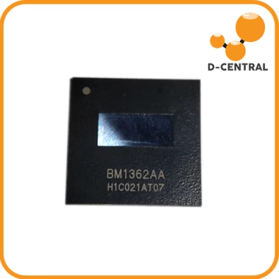
The open-source mining hardware movement is a direct response. Projects like the Bitaxe take a fundamentally different approach: rather than designing custom ASIC chips from scratch, they build open-source mining boards around existing ASIC chips sourced from commercial miners. The Bitaxe Supra, for example, uses a single BM1366 chip (the same chip found in the Antminer S19k Pro), running it at optimized voltages on a compact PCB designed for solo mining.
This approach turns the ASIC supply chain on its head:
- No foundry relationship needed: The chips already exist — sourced from production overruns, salvaged from decommissioned miners, or purchased through component markets.
- Open hardware design: The PCB schematics, firmware, and mechanical designs are published openly. Anyone can manufacture a Bitaxe.
- Accessible form factor: A single-chip board that runs on a 5V barrel jack (5.5×2.1mm DC — not USB-C, which is for firmware flashing only) and connects to your home WiFi. No industrial infrastructure required.
- Solo mining focus: These devices run on solo mining pools, giving every operator a direct shot at finding a block and earning the full 3.125 BTC reward.
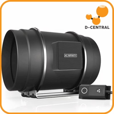
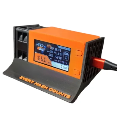
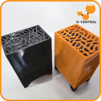
D-Central Technologies has been a pioneer in the Bitaxe ecosystem since its earliest days. We created the original Bitaxe Mesh Stand — the first company to manufacture it — and have developed many of the leading Bitaxe solutions including custom heatsinks for both the standard Bitaxe and the Bitaxe Hex, custom cases, and a full range of accessories. We stock every Bitaxe variant (Supra, Ultra, Hex, Gamma, GT) along with the complete Nerd/open-source lineup (Nerdminer, NerdNOS, NerdAxe, NerdQAxe). Visit the Bitaxe Hub for the definitive guide to every model and accessory.
What ASIC Design Means for Repair and Maintenance
If you operate mining hardware, understanding ASIC chip design is not academic — it directly impacts your ability to maintain and repair your machines. Here is what you need to know from the repair bench perspective.
Why Chips Fail
Mining ASICs operate under extreme conditions: sustained high current, elevated temperatures, and continuous 24/7 operation. Common failure modes directly tied to chip design and manufacturing include:
- Electromigration: Sustained high-current operation gradually moves metal atoms in the chip’s interconnects, eventually causing open circuits. This is a physics-level degradation that accelerates with temperature and current density.
- Thermal cycling fatigue: Repeated heating and cooling cycles (from power cycling or ambient temperature swings) stress the solder joints between the ASIC package and the hashboard PCB, eventually cracking them.
- Voltage regulator failure: The ultra-low voltages used by modern ASICs (0.25-0.40V) require extremely precise voltage regulation. If a VRM on the hashboard drifts, chips downstream can be overvoltaged and damaged, or undervoltaged and non-functional.
- Manufacturing defects: Latent defects that passed initial testing but manifest after extended operation. These are more common in chips from early production runs on new process nodes.
Repair at the Chip Level
At D-Central’s repair facility, we diagnose and repair hashboards at the individual chip level. This involves:
- Chain detection testing: Communicating with each ASIC chip in the hash chain to identify which chip has failed or is responding abnormally.
- Thermal imaging: Using infrared cameras to identify chips running abnormally hot (shorted) or cold (open circuit / non-functional).
- Chip replacement: Removing the failed ASIC using hot-air rework stations and soldering a replacement chip. For BGA packages, this requires precise temperature profiles to avoid damaging surrounding components.
- Domain voltage testing: Verifying that each voltage domain on the hashboard delivers the correct voltage to its group of ASIC chips.
Understanding the ASIC’s package type, pin configuration, thermal requirements, and electrical specifications is essential for proper repair work. A technician who understands chip design can diagnose problems faster, avoid creating secondary damage during repair, and determine whether a hashboard is worth repairing or has suffered fundamental failure. If your machines need professional diagnosis, D-Central’s ASIC repair service handles everything from individual chip replacement to full hashboard restoration.
The Future of Bitcoin Mining ASICs
Where does ASIC design go from here? Several trends are shaping the next generation of mining silicon:
Approaching Physical Limits
At 3nm and below, we are approaching fundamental physical constraints. Quantum tunneling effects become significant at these scales, leakage current increases, and each further reduction in feature size yields diminishing returns in efficiency improvement. The era of easy 30-50% generational efficiency gains may be ending.
Advanced Packaging Takes Over
When shrinking the transistor stops delivering big gains, chipmakers pivot to advanced packaging. Techniques like chiplet architectures (multiple small dies connected in a single package), 3D stacking, and advanced thermal interfaces can improve overall system efficiency without requiring a smaller process node.
Immersion and Liquid Cooling Co-Design
ASICs designed specifically for immersion cooling can run at higher power densities since heat removal is dramatically more efficient. This co-design approach — optimizing the chip, package, and cooling system together — unlocks performance that air-cooled designs cannot achieve. Bitmain’s Antminer S21 Hydro line is an early example of this direction.
Decentralization of Manufacturing
The open-source hardware movement — including Bitaxe and the broader community of open mining hardware projects — is working to reduce dependency on a small number of ASIC manufacturers. While designing a competitive custom mining ASIC remains expensive, the ecosystem of open-source boards using commodity ASIC chips continues to grow and mature. Every home miner running a Bitaxe or NerdAxe is a node of manufacturing decentralization.
Energy Efficiency as the Survival Metric
With the block reward now at 3.125 BTC post-halving and difficulty above 110T, only the most efficient hardware survives in competitive mining. ASIC designers are pushing every available technique — lower operating voltages, optimized SHA-256 core architectures, advanced process nodes, and better thermal design — to extract more hashes per joule. For home miners, this means newer machines are not just faster, they are fundamentally more economical to operate.
Why This Matters for Home Miners
You do not need to design your own ASIC to benefit from understanding how they work. Here is what ASIC design knowledge gives you as a home miner:
- Better purchasing decisions: Understanding process nodes and efficiency metrics helps you evaluate whether a new miner justifies its price premium over the previous generation.
- Smarter overclocking and underclocking: Knowing how voltage affects chip behavior lets you tune your miners for your specific electricity cost and thermal constraints.
- Informed repair decisions: When a hashboard fails, understanding chip-level failure modes helps you assess whether repair is worthwhile or if the board is beyond economical recovery.
- Dual-purpose mining insight: Knowing that 100% of electrical energy consumed by an ASIC becomes heat lets you design effective mining heater setups with confidence in the physics.
- Decentralization participation: Understanding open-source mining hardware like the Bitaxe lets you participate in decentralizing Bitcoin’s hash rate — the Bitaxe Hub is your starting point.
The art and science of ASIC design is ultimately the art and science of securing the Bitcoin network. Every transistor in every mining chip exists to make the network more secure, more resistant to attack, and more decentralized. Whether you are running a single Bitaxe on your desk or a rack of S21s in your garage, you are part of that security infrastructure.
Need help choosing, configuring, or repairing mining hardware? D-Central’s mining consulting team has been helping home miners since 2016. From your first Bitaxe to a full home mining operation, we have the experience to guide you. Browse our full selection of miners and accessories in the D-Central shop.
Frequently Asked Questions
What is an ASIC and why is it used in Bitcoin mining?
An Application-Specific Integrated Circuit (ASIC) is a chip designed to perform one specific task. In Bitcoin mining, ASICs are engineered exclusively to compute SHA-256 hashes — the cryptographic function used in Bitcoin’s Proof-of-Work consensus. Because every transistor is dedicated to this single function, mining ASICs achieve vastly superior efficiency compared to CPUs, GPUs, or FPGAs. All serious Bitcoin mining in 2026 runs on ASICs.
How does the semiconductor process node affect mining efficiency?
The process node (measured in nanometers) determines the size of transistors on the chip. Smaller nodes (e.g., 5nm, 3nm) allow more transistors per mm² of silicon, enable lower operating voltages, and reduce power consumption per hash. Each generational jump typically delivers 30-50% efficiency improvement. The latest mining ASICs on 3nm process nodes achieve approximately 13-15 J/TH, compared to ~98 J/TH for the 16nm chips in the Antminer S9 era.
Why do some miners of the same model have different efficiency ratings?
This is primarily due to silicon binning. After fabrication, each chip is tested and graded based on performance. Top-bin chips achieve the highest frequencies at the lowest voltages and go into premium models. Lower-bin chips require more voltage for the same hashrate or run at lower speeds, and are used in standard or budget tiers. The underlying chip design is identical — the difference is manufacturing quality variation.
Can I design my own Bitcoin mining ASIC?
Designing a competitive custom mining ASIC requires tens of millions of dollars in development costs, deep semiconductor expertise, and relationships with advanced foundries like TSMC or Samsung. However, the open-source mining hardware movement offers an alternative: projects like the Bitaxe build open-source mining boards around existing ASIC chips, making the technology accessible to individual builders and small manufacturers. D-Central stocks the full range of open-source miners — visit the Bitaxe Hub for details.
What causes ASIC chips to fail in mining machines?
Common failure modes include electromigration (metal atoms in chip interconnects shifting under sustained high current), thermal cycling fatigue (solder joint cracking from repeated temperature swings), voltage regulator failures on the hashboard causing over/under-voltage conditions, and latent manufacturing defects. Continuous 24/7 operation at high temperatures accelerates all of these mechanisms. Professional ASIC repair services can diagnose and replace individual failed chips.
How do open-source miners like the Bitaxe use commercial ASIC chips?
Open-source miners like the Bitaxe use individual ASIC chips sourced from commercial miners or component markets, mounting them on custom-designed open-source PCBs. The Bitaxe Supra, for example, runs a single BM1366 chip (the same chip used in the Antminer S19k Pro) on a compact board powered by a 5V barrel jack. This approach democratizes mining hardware without requiring custom chip fabrication. The full PCB designs, firmware, and schematics are publicly available.
Is there a future beyond silicon for Bitcoin mining?
Current ASIC designs are approaching fundamental physical limits at 3nm and below, where quantum tunneling and leakage current constrain further gains. The industry is shifting focus to advanced packaging (chiplets, 3D stacking), co-designed cooling systems (immersion-optimized chips), and architectural optimizations within existing process nodes. Entirely new computing substrates are theoretically possible but remain decades from commercial viability. For the foreseeable future, silicon ASIC efficiency improvements will continue through incremental innovation.