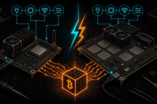
The BM1397 is not just another chip — it is the silicon backbone of an entire generation of Bitcoin miners that helped decentralize hashrate across the globe. Developed by Bitmain and manufactured on TSMC’s 7nm FinFET process, this ASIC chip powers the Antminer 17 series (S17, S17 Pro, S17+, T17, T17+) and remains one of the most repairable, hackable, and well-documented mining chips ever produced.
At D-Central, we have replaced, reflowed, and diagnosed thousands of BM1397 chips across our ASIC repair bench. This is not theoretical knowledge — it is hard-won, solder-under-the-fingernails expertise. This guide breaks down the BM1397’s architecture, communication protocol, register map, and tuning parameters so you can understand exactly what is happening inside your miner — and how to push it further.
Whether you are a home miner troubleshooting a dead hashboard or a repair technician diagnosing chain communication failures, this is the reference you need.
BM1397 Architecture: What Makes This Chip Tick
The BM1397 is an Application-Specific Integrated Circuit (ASIC) purpose-built for one task: computing SHA-256 double hashes as fast and efficiently as possible. That is the proof-of-work algorithm that secures the Bitcoin network — currently running at over 800 EH/s globally with a block reward of 3.125 BTC.
Built on TSMC’s 7nm FinFET node, the BM1397 represented a generational leap in energy efficiency when it launched. Each chip contains hundreds of hashing cores operating in parallel, connected in a daisy-chain configuration on each hashboard. A typical Antminer S17 hashboard carries dozens of these chips, all working in concert.
| Specification | BM1397 |
|---|---|
| Manufacturer | Bitmain |
| Process Node | TSMC 7nm FinFET |
| Algorithm | SHA-256 (double hash) |
| Used In | Antminer S17, S17 Pro, S17+, T17, T17+ |
| Default UART Baud | 115200 bps (8N1) |
| Input Clock (CLKI) | 25 MHz |
| AsicBoost Support | Yes (Multi-Midstate via MMEN bit) |
| Chain Configuration | Daisy-chain via UART (CI/RO pins) |
The BM1397 also supports AsicBoost through its Multi-Midstate Enable (MMEN) bit — a legitimate optimization technique that reduces the number of SHA-256 computations needed per hash attempt. Understanding this chip at the register level is the difference between running a miner and truly mastering it.
Chip Address and Enumeration: Talking to Individual Chips
Every BM1397 chip on a hashboard shares the same UART bus. When power is applied and the chips are reset, every single chip defaults to address 0. If you sent a command to address 0, the entire chain would execute it simultaneously. That is useful for broadcast commands but useless for targeted diagnostics or per-chip tuning.
The solution is enumeration — assigning a unique logical address to each chip in sequence. Here is how the process works:
Step 1 — Chain Inactive Command. A special command tells all chips to stop relaying commands down the chain. This isolates the first chip so it alone receives the next instruction.
Step 2 — Set Chip Address. With the chain frozen, a Set Chip Address command assigns a new address to the first chip (the only one still at address 0). That chip accepts the address and starts relaying again.
Step 3 — Repeat. The process repeats. Each iteration, the previously-addressed chips ignore the command (their address is no longer 0), and the next unaddressed chip in the chain picks it up. This continues until every chip on the board has a unique address.
Addresses do not need to be sequential. In practice, they are often assigned with an increment of 4 or 8. This is not arbitrary — it divides the 32-bit nonce space evenly across chips. Each chip adds its own address offset to the nonce it is hashing, which guarantees that no two chips duplicate work. Efficient nonce partitioning is fundamental to maximizing hashrate per watt.
If you are diagnosing a hashboard that shows partial chains or missing chips, a failed enumeration is often the root cause. A single chip with a broken UART path will prevent every chip downstream from receiving an address — and those chips produce zero hashes.
Hash Rate Calculation: Where the Numbers Come From
Hash rate is the metric that matters — it measures how many SHA-256 double hashes the chip computes per second. On the BM1397, the hash rate is derived from the PLL0 (Phase-Locked Loop 0) clock frequency.
The hash rate register sits at address 0x04 with a reset value of 0x80000000. The value is expressed in units of 224 hashes per second.
But the raw hash rate number is meaningless without context. What actually determines your effective hashrate is the PLL0 clock frequency, which is fully configurable through the chip’s registers.
PLL0: The Master Clock
PLL0 is the base clock from which the BM1397 derives its hashing frequency. It lives at register address 0x08 with a reset value of 0xC0600161. The frequency is calculated with this formula:
fPLL0 = fCLKI x FBDIV / (REFDIV x POSTDIV1 x POSTDIV2)
| Parameter | Description |
|---|---|
fCLKI |
Input clock frequency (25 MHz from the control board) |
FBDIV |
Feedback divider — the multiplication factor for the PLL |
REFDIV |
Reference divider — scales down the input frequency before multiplication |
POSTDIV1 |
First post-divider (must be greater than or equal to POSTDIV2) |
POSTDIV2 |
Second post-divider |
By adjusting FBDIV, REFDIV, POSTDIV1, and POSTDIV2, you directly control the chip’s hashing clock — and therefore its hashrate and power consumption. This is how firmware authors and overclockers tune Antminer performance. Higher FBDIV values push more hashes per second but draw more current and generate more heat. Finding the sweet spot for your cooling setup is the art of mining optimization.
Core Registers: The Control Panel
The BM1397 exposes a set of core registers that give you granular control over chip behavior. These are accessed via the Read Register and Write Register UART commands.
| Register ID | Name | Function |
|---|---|---|
| 0 | Clock Delay Ctrl | Frequency tuning (CCDLY_SEL, PWTH_SEL) and AsicBoost enable (MMEN) |
| 1 | Process Monitor Ctrl | Reads per-core process parameters for binning and diagnostics |
| 2 | Process Monitor Data | Holds data read by the process monitor |
| 3 | Core Error | Error codes for core-level faults |
| 4 | Core Enable | Enable or disable individual hashing cores |
| 5 | Hash Clock Control | Controls the hashing clock — the core of the mining engine |
| 6 | Hash Clock Counter | Counts hash clock cycles for performance measurement |
| 7 | Sweep Clock Control | Controls the sweep clock used during the mining process |
The Core Enable register (ID 4) deserves special attention. When a chip has defective cores — common in aging or heat-damaged chips — disabling those cores via this register prevents them from submitting bad nonces that waste bandwidth and trigger hardware errors in the miner’s control software. This is a standard technique in professional ASIC repair and chip-level diagnostics.
UART Communication Protocol: Speaking the Chip’s Language
All communication with the BM1397 happens over UART (Universal Asynchronous Receiver/Transmitter) — a serial protocol. The chip uses four critical pins for communication:
| Pin | Name | Function |
|---|---|---|
| NRSTI | Negated Reset Input | Hardware reset when pulled LOW |
| CLKI | Clock Input | 25 MHz reference clock, propagated to CLKO |
| CI | Command Input | UART RX — receives commands from the control board |
| RO | Response Output | UART TX — sends responses (nonces, register data) back |
The BI (Busy Input) pin must be pulled low to allow communication. The default UART configuration is 115200 baud, 8 data bits, no parity, 1 stop bit (115200 8N1).
Command Structure: Every command begins with the preamble 0x55 0xAA, followed by a TYPE field. TYPE 1 sends a mining job (block header + nonce range). TYPE 2 sends a chip command (address assignment, register read/write). TYPE 3 is the Chain Inactive command used during enumeration. The ALL bit determines whether the command targets a single chip or the entire chain.
Response Structure: Responses begin with 0xAA 0x55. TYPE 0 is a command response (returning register data). TYPE 4 is a nonce response — the chip found a valid nonce and is reporting it back to the control board.
When a hashboard reports communication errors or fails to initialize, the UART bus is the first place to investigate. Cold solder joints on CI/RO pins, broken traces between chips, and corroded connectors are all common failure modes that our repair technicians see regularly at D-Central.
Setting the Baud Rate: Faster Communication for Higher Hashrate
The default 115200 bps baud rate works fine for initialization and low-speed operation, but high-hashrate configurations require faster chip-to-controller communication. More hashes per second means more nonce responses flowing back up the chain, and the UART bus needs the bandwidth to handle it.
The baud rate adjustment process is straightforward but must be done carefully:
1. Send the Set Baud Rate command to all chips on the chain with the desired new rate.
2. Switch your controller’s UART to match the new baud rate immediately after sending the command.
3. Verify with a register read to confirm the chips are responding at the new speed.
4. If communication fails, a hardware reset (NRSTI pin LOW) will revert all chips to the default 115200 bps, and you can try again.
Pushing the baud rate too high without adequate signal integrity — clean traces, good termination, minimal EMI — will result in corrupted commands and dropped nonces. This is another area where board-level repair knowledge becomes critical.
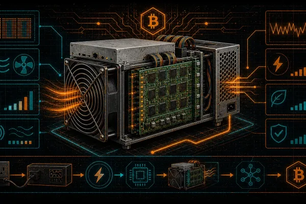
Why This Matters for Home Miners and Repair Technicians
The BM1397 powers millions of mining machines still running today. Even as newer chip generations like the BM1398 and BM1370 roll out, the Antminer 17 series remains a workhorse — especially for home miners and Bitcoin space heater builds where efficiency per dollar matters more than peak performance.
Understanding the BM1397 at this level lets you:
Diagnose hashboard failures by identifying which chip in the chain is breaking communication — saving you from replacing an entire board when one chip needs rework.
Optimize clock frequencies through PLL0 tuning to find the best hashrate-to-power ratio for your specific setup and ambient temperature.
Disable defective cores to salvage partially-damaged chips instead of scrapping them.
Validate repairs by reading chip registers after rework to confirm proper communication before reassembling the miner.
This is what we mean by “Bitcoin Mining Hackers.” The knowledge to crack open a miner, speak its chip’s language at the register level, and bend the hardware to your will — that is sovereignty over your own mining operation.
If you need professional-grade repair on Antminer 17 series machines or any other ASIC hardware, D-Central’s ASIC repair service has you covered. We have been repairing miners since 2016 from our facility in Montreal, Quebec, and we stock BM1397 chips and hashboard components for the full Antminer 17 lineup. Check our shop for replacement parts, or explore the Bitaxe Hub if you are looking to get into open-source solo mining with hardware you fully control.
Every hash counts. Every chip matters. Know your hardware.
Frequently Asked Questions
What is the BM1397 chip and which miners use it?
The BM1397 is a 7nm ASIC chip designed by Bitmain specifically for SHA-256 Bitcoin mining. It powers the Antminer 17 series, including the S17, S17 Pro, S17+, T17, and T17+. Each hashboard in these miners contains dozens of BM1397 chips operating in a daisy-chain configuration.
How does chip enumeration work on the BM1397?
All chips reset to address 0. A Chain Inactive command freezes relay, then a Set Chip Address command assigns a unique address to the first chip. The process repeats for each chip in sequence. Addresses are typically incremented by 4 or 8 to partition the 32-bit nonce space evenly across chips.
What is PLL0 and how does it affect hashrate?
PLL0 (Phase-Locked Loop 0) is the master clock that determines the BM1397’s hashing frequency. Its frequency is calculated as fPLL0 = fCLKI x FBDIV / (REFDIV x POSTDIV1 x POSTDIV2). Increasing FBDIV raises the hashrate but also increases power consumption and heat output.
What UART settings does the BM1397 use?
The default UART configuration is 115200 baud, 8 data bits, no parity, 1 stop bit (115200 8N1). For higher-hashrate operation, the baud rate can be increased through a Set Baud Rate command, but signal integrity must support the faster communication speed.
Can I disable individual cores on a BM1397 chip?
Yes. The Core Enable register (ID 4) allows you to enable or disable individual hashing cores. This is a common repair technique — disabling defective cores prevents bad nonce submissions and hardware errors, effectively salvaging a chip that would otherwise need full replacement.
Does the BM1397 support AsicBoost?
Yes. The Clock Delay Control register (ID 0) contains the MMEN (Multi-Midstate Enable) bit, which activates AsicBoost. This optimization reduces the number of SHA-256 computations per hash attempt, improving efficiency without increasing power draw.
What causes BM1397 chip failures?
The most common failure modes are thermal damage from inadequate cooling, cold solder joints from thermal cycling, electrostatic discharge (ESD), and power delivery issues. Symptoms include missing chips during enumeration, UART communication errors, and abnormally low hashrate on specific chains. Professional diagnosis involves register reads and UART signal tracing.
Where can I get BM1397 chips and Antminer 17 series repairs?
D-Central Technologies stocks BM1397 replacement chips and hashboard components. Our ASIC repair service in Montreal, Quebec has been servicing mining hardware since 2016. Visit d-central.tech/asic-repair for repair services or d-central.tech/shop for parts.
 Bitaxe Heatsink — High-Performance Aluminum Cooler for Bitaxe & Nerdaxe Gamma / Supra / Ultra — Silent Operation & Stable Overclocking" width="80" height="80" loading="lazy" style="width:80px;height:80px;object-fit:contain;border-radius:6px;background:#1A1A1A;flex-shrink:0;">
Shop Heatsinks
Bitaxe Heatsink — High-Performance Aluminum Cooler for Bitaxe & Nerdaxe Gamma / Supra / Ultra — Silent Operation & Stable Overclocking" width="80" height="80" loading="lazy" style="width:80px;height:80px;object-fit:contain;border-radius:6px;background:#1A1A1A;flex-shrink:0;">
Shop Heatsinks