Every Bitcoin block mined is a feat of silicon engineering. The SHA-256 hash function that secures the Bitcoin network does not care about marketing decks or brand loyalty. It cares about one thing: how many hashes per joule your hardware can produce. And that number is dictated almost entirely by the lithography process used to fabricate the ASIC chips inside your miner.
Since D-Central Technologies entered the Bitcoin mining space in 2016, we have watched lithography drive the single most consequential trend in mining hardware: the relentless march from 130nm process nodes down to 3nm and soon 2nm. Each shrink does not merely make chips smaller. It rewrites the economics of mining, changes who can profitably mine, and reshapes the decentralization of hashrate across the network.
This is a deep technical walkthrough of how semiconductor lithography improvements have transformed Bitcoin mining efficiency, where the technology stands in 2025-2026, and what the next generation of process nodes means for home miners and the broader network.
What Lithography Actually Does Inside Your ASIC Miner
Lithography is the process of using light to etch transistor patterns onto silicon wafers. Think of it like a microscopic stencil: a mask containing the circuit design is projected onto a photoresist-coated silicon wafer, and the exposed areas are chemically etched to create the transistor structures that perform SHA-256 computations.
The “nanometer” measurement (nm) in process node names refers to the feature size of the transistors. Smaller features mean:
- More transistors per chip — higher compute density, more SHA-256 cores per die
- Lower voltage operation — transistors switch faster at lower energy cost
- Reduced heat output — less energy wasted as thermal dissipation
- Higher yields per wafer — more functional chips from the same silicon disc
For Bitcoin miners, these translate directly into the metric that matters most: joules per terahash (J/TH). A lower J/TH means your miner produces more hashrate per watt of electricity consumed. When your electricity bill is your largest operational cost, J/TH is the number that determines whether you mine at a profit or at a loss.
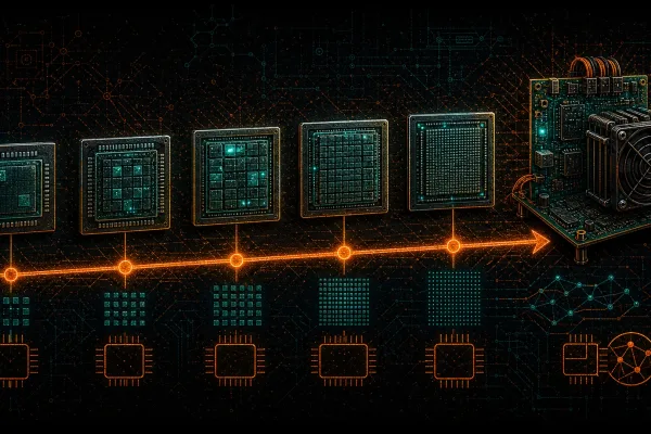
The Lithography Timeline: From 130nm to 3nm
The history of Bitcoin ASIC development is essentially a history of chasing smaller process nodes. Each generation brought dramatic efficiency gains that reshaped the mining landscape.
| Era | Process Node | Representative Miner | Chip | Efficiency (J/TH) | Year |
|---|---|---|---|---|---|
| Genesis | 130nm | Avalon 1 | A3256 | ~9,000 | 2013 |
| Early ASIC | 55nm | Antminer S3 | BM1382 | ~700 | 2014 |
| Maturation | 28nm | Antminer S5/S7 | BM1384/BM1385 | ~250-170 | 2015 |
| Golden Age | 16nm | Antminer S9 | BM1387 | ~98 | 2016 |
| 7nm Revolution | 7nm | Antminer S17/S19 | BM1397/BM1398 | ~40-30 | 2019-2020 |
| 5nm Era | 5nm | Antminer S19 XP / S21 | BM1366/BM1370 | ~21-15 | 2022-2024 |
| Current Edge | 3nm | Triple-1 Kamikaze III / Block-ePIC | Kamikaze III | ~10 | 2025 |
| Next Gen | 2nm | Bitmain (expected) | TBA | ~5-7 (target) | 2026 |
That table tells a staggering story. From roughly 9,000 J/TH in 2013 to under 15 J/TH in 2024, the industry achieved a 600x improvement in mining efficiency in just over a decade. Most of that improvement came directly from lithography advances.
The 16nm Watershed: How the Antminer S9 Changed Everything
The jump to 16nm in 2016 with the BM1387 chip was arguably the most consequential lithography leap in Bitcoin mining history. The Antminer S9 delivered approximately 14 TH/s at around 98 J/TH, a figure so efficient relative to its era that the machine remained viable for years after its release.
At D-Central, we have repaired thousands of S9 boards and watched these machines serve home miners and commercial operations for the better part of a decade. The S9 became the backbone of our Bitcoin Space Heater lineup because its heat output and form factor make it ideal for dual-purpose mining and heating.
The 16nm node was where Bitcoin mining became industrially efficient. Prior nodes (28nm, 55nm) were too power-hungry for anything but cheap-electricity operations. The S9 opened the door for home miners running off residential power, and that door has never closed.
7nm and the Race for Sub-50 J/TH
The transition from 16nm to 7nm, primarily on TSMC’s N7 process, brought the next wave of efficiency gains. Bitmain’s BM1397 chip (Antminer S17 series) and the subsequent BM1398 (S19 series) pushed efficiency below 30 J/TH for the first time.
This generation also marked the rise of MicroBT as a serious competitor, with their Whatsminer M30S series achieving comparable efficiency on Samsung’s 8nm process. The competition was healthy for miners: two major foundry partnerships (TSMC and Samsung) driving innovation in parallel.
For the network, 7nm meant that the total hashrate could grow dramatically without proportional energy growth. This is the counter-narrative to the perennial “Bitcoin uses too much energy” criticism. Lithography improvements mean the network secures more value with less energy per hash, every single generation.
5nm: The Current Workhorse Generation
TSMC’s 5nm process (N5) is the node that powers the current generation of high-efficiency miners. Bitmain’s BM1366 chip brought the Antminer S19 XP to approximately 21.5 J/TH, and the more recent BM1370 in the S21 series pushed that further to around 15 J/TH.
At 5nm, the engineering challenge shifts. You cannot just shrink transistors and expect linear efficiency gains. Chip designers must contend with:
- Increased leakage current — at smaller nodes, transistors “leak” more electricity even when not switching
- Voltage floor limitations — there is a minimum operating voltage below which transistors become unreliable
- Manufacturing cost escalation — 5nm wafers cost significantly more than 7nm wafers
- Design complexity — more transistors per chip means more complex verification and testing
Despite these challenges, 5nm established the efficiency range (13-21 J/TH) that defines commercially competitive mining in 2025. If your hardware operates above 25 J/TH, you are fighting an uphill battle against operators running 5nm machines, especially post-halving.
The Open-Source 5nm Revolution
One of the most exciting developments in the 5nm era is not happening in Bitmain’s or MicroBT’s factories. It is happening in the open-source community. The Bitaxe project takes production ASIC chips like the BM1366 and BM1370 and places them on open-source PCB designs that anyone can manufacture, modify, and improve.
D-Central has been a pioneer in the Bitaxe ecosystem since its earliest days. We created the original Bitaxe Mesh Stand, developed leading heatsink solutions for both the standard Bitaxe and the Bitaxe Hex, and stock every variant: Supra, Ultra, Hex, Gamma, and GT. The Bitaxe Gamma, built around the BM1370 chip from the Antminer S21 Pro, puts 5nm-class solo mining in the hands of individual Bitcoiners for a fraction of the cost of a full ASIC.
This is what lithography advancement means for decentralization. When cutting-edge silicon becomes accessible through open-source designs, hashrate distribution improves. Every home miner running a Bitaxe on their desk is a node of resistance against mining centralization.
3nm: The Bleeding Edge in 2025
The 3nm process node represents the current frontier of Bitcoin mining ASIC development, with several players pushing the boundaries:
Triple-1 Kamikaze III
Japanese ASIC designer Triple-1 has developed the Kamikaze III on TSMC’s 3nm process, achieving a remarkable 10.45 J/TH through proprietary sub-threshold operation techniques. Sub-threshold design operates transistors at voltages (as low as 0.26V for the Kamikaze III) below their normal switching threshold, dramatically reducing power consumption at the cost of reduced clock speeds. For SHA-256 mining, where massive parallelism matters more than clock speed, this trade-off is ideal.
Block and ePIC Blockchain
Block (formerly Square), led by Jack Dorsey, has partnered with ePIC Blockchain to develop 3nm mining ASICs. Their stated goal is to make mining more accessible and decentralized, aligning with the broader open-source mining movement.
Bitdeer SEAL Series
Bitdeer’s SEALMINER roadmap provides a clear view of how lithography drives their product strategy. Their SEAL02 chip achieved 13.5 J/TH on an advanced node, while the SEAL04 chip is targeting 5-7 J/TH at the chip level. Mass production of SEAL04-based miners is expected in early 2026.
| Company | Chip | Process | Efficiency (J/TH) | Status (2025) |
|---|---|---|---|---|
| Bitmain | BM1370 | 5nm | ~15 | Shipping (S21 XP) |
| MicroBT | M60S++ chip | 5nm | ~16 | Shipping |
| Bitdeer | SEAL02 | Advanced node | ~13.5 | Production |
| Triple-1 | Kamikaze III | 3nm TSMC | ~10.5 | Tapeout complete |
| Block/ePIC | Proto chip | 3nm | TBA | Development |
| Bitdeer | SEAL04 | Advanced node | ~5-7 (target) | Testing, mass production Q1 2026 |
EUV Lithography: The Technology Making Sub-5nm Possible
Everything below 7nm depends on Extreme Ultraviolet (EUV) lithography, a technology that took decades and billions of dollars to commercialize. Understanding EUV is essential to understanding why modern mining ASICs are so efficient and why further improvements are becoming harder.
How EUV Works
Traditional lithography uses deep ultraviolet (DUV) light at 193nm wavelength. At sub-7nm feature sizes, 193nm light is simply too coarse to draw fine enough patterns. EUV uses 13.5nm wavelength light, generated by blasting tiny tin droplets with a high-power laser to create plasma that emits EUV radiation.
The engineering challenges are immense:
- Light source power: EUV photons are absorbed by almost everything, including air. The entire optical path must operate in a near-vacuum, and generating sufficient EUV intensity requires enormous laser power.
- Reflective optics: Because EUV is absorbed by glass lenses, the system uses multilayer mirrors (alternating layers of molybdenum and silicon) that reflect only about 70% of incident EUV light per surface. With six mirrors in the optical path, total throughput is roughly 12%.
- Mask defects: At 13.5nm wavelength, even atomic-scale imperfections on the photomask can print as defects on the wafer.
- Stochastic effects: At extreme resolutions, the random nature of individual photon absorption creates variability in feature sizes, leading to potential transistor failures.
Only one company on Earth manufactures EUV lithography systems: ASML, headquartered in the Netherlands. Their current-generation TWINSCAN NXE systems cost over $200 million each. The next-generation High-NA EUV systems (TWINSCAN EXE series) cost roughly $380 million per unit and are required for 2nm and below.
Why EUV Costs Matter for Miners
EUV’s extraordinary cost is baked into every wafer produced at 5nm and below. This is why the price of leading-edge ASICs has not fallen as quickly as efficiency has improved. A 3nm wafer from TSMC costs roughly two to three times what a 7nm wafer costs. For ASIC manufacturers, the calculus is straightforward: the efficiency gains must justify the silicon cost premium, or they cannot offer competitive pricing.
TSMC has signaled 3-5% annual price increases for sub-5nm nodes beginning in 2026, which will further pressure ASIC pricing. For miners, this means that the cheapest hardware is not always the most profitable hardware. The efficiency advantage of newer lithography can more than offset a higher purchase price, depending on your electricity rate.
2nm and Beyond: What Is Coming in 2026
TSMC’s N2 (2nm) process is the next major node, with volume production expected to ramp to 60,000 wafers per month by Q4 2026. Reports indicate that both Apple and Bitmain are among the primary customers for N2 capacity. If confirmed, this means we could see 2nm Bitcoin mining ASICs entering the market in late 2026 or early 2027.
At 2nm, TSMC is transitioning from FinFET transistor architecture to Gate-All-Around (GAA) nanosheet transistors. GAA provides better electrostatic control over the transistor channel, enabling:
- Lower operating voltages without sacrificing performance
- Reduced leakage current compared to FinFET at equivalent feature sizes
- Greater design flexibility for optimizing power versus speed trade-offs
For Bitcoin mining, where the workload is embarrassingly parallel and clock speed matters less than power efficiency, GAA transistors could unlock significant J/TH improvements. Bitdeer’s SEAL04 chip, targeting 5-7 J/TH, likely leverages these architectural advantages.
High-NA EUV lithography from ASML is also entering production for sub-2nm nodes. Intel has installed the TWINSCAN EXE:5200B for its upcoming 14A node (roughly 1.4nm equivalent), with TSMC and Samsung planning similar deployments. These systems enable finer patterning with fewer multi-exposure steps, improving both yield and throughput.
Why Lithography Gains Matter for Bitcoin Decentralization
Here is the point that most technical analyses miss: lithography improvements do not just make mining cheaper. They reshape who can mine.
When the Antminer S9 brought 16nm efficiency to market in 2016, it enabled a generation of home miners who could not have operated profitably on 28nm hardware. When 5nm chips appeared in the Bitaxe ecosystem, solo mining became viable for individual Bitcoiners running a single chip on their desk.
Each lithography generation lowers the watts-per-hash floor. This means:
- Home miners can run more hashrate within residential electrical limits (15A or 20A circuits)
- Renewable energy operators can extract more Bitcoin value from the same solar panel or wind turbine output
- Dual-purpose miners running Bitcoin Space Heaters get more hashrate from the same thermal output
- Solo miners get more lottery tickets per kilowatt-hour, improving their odds of finding a block
This is why we care so deeply about lithography at D-Central. We are not chip designers. We are Bitcoin Mining Hackers who take the silicon that TSMC and Samsung produce and put it into the hands of individuals. Every lithography shrink that makes ASICs more efficient is a shrink that makes mining more decentralized.
The Efficiency Wall: Are We Approaching Physical Limits?
A question we hear frequently: is there a hard floor on mining efficiency? The answer is yes, but we are not there yet.
The theoretical minimum energy to compute a SHA-256 hash is governed by the Landauer limit, which dictates the minimum energy required to erase one bit of information. For practical SHA-256 mining, this theoretical floor is many orders of magnitude below current hardware. The real limits are engineering constraints, not physics:
- Interconnect resistance: As wires shrink, their electrical resistance increases, generating heat and limiting speed
- Quantum tunneling: Below approximately 3nm, electrons can tunnel through transistor gates, causing uncontrollable leakage
- Manufacturing economics: Each node shrink costs more to develop and produce, requiring larger production volumes to amortize
- Packaging and cooling: Chip-level efficiency gains can be offset by system-level thermal management challenges
Industry experts estimate that the practical J/TH floor for SHA-256 ASICs is somewhere in the range of 2-5 J/TH, achievable with 2nm or sub-2nm process technology combined with aggressive voltage optimization techniques like Triple-1’s sub-threshold approach. We may reach this range within the next two to three years.
After that, further improvements will come from architectural innovations (3D chip stacking, advanced packaging, novel cooling techniques) rather than transistor shrinks. The era of easy efficiency gains from lithography is entering its final chapters.
What This Means for Your Mining Operation
Understanding lithography is not academic for miners. It directly informs hardware purchasing decisions:
| Your Situation | Recommended Hardware Generation | Reasoning |
|---|---|---|
| Low electricity cost (<$0.05/kWh) | 7nm or 5nm (S19/S21 series) | Cheap power offsets lower efficiency; used 7nm hardware offers excellent ROI |
| Moderate electricity ($0.05-0.10/kWh) | 5nm (S21 XP class) | Need sub-15 J/TH to maintain margins post-halving |
| High electricity (>$0.10/kWh) | Latest 5nm or 3nm when available | Only leading-edge efficiency keeps you profitable |
| Home heating integration | 16nm (S9 Space Heaters) or 7nm | Heat output is the primary value; mining revenue is a bonus |
| Solo mining / lottery mining | 5nm open-source (Bitaxe Gamma) | Maximize hashes per watt on a residential circuit; every hash counts |
The critical insight is that lithography generation determines the useful lifespan of your hardware. An S9 (16nm) purchased in 2016 mined profitably for four to six years before electricity costs overtook revenue at typical rates. An S21 XP (5nm) purchased in 2024 is likely to have a similarly long productive life because the gap to 3nm and 2nm, while meaningful, is narrower than the gap from 16nm to 5nm was.
D-Central’s Role in the Lithography Ecosystem
We do not fabricate silicon. What we do is extend the life, accessibility, and utility of every lithography generation:
- ASIC Repair: Our repair service keeps older-generation hardware running. Replacing a failed BM1387 chip on an S9 hashboard or a BM1397 on an S17 board gives that silicon a second life.
- Open-Source Mining: Through the Bitaxe ecosystem, we make 5nm chips accessible as individual units for solo mining, not locked behind multi-thousand-dollar ASIC machines.
- Dual-Purpose Integration: Our Bitcoin Space Heaters transform older 16nm and 7nm ASICs into home heating appliances that mine Bitcoin as a byproduct.
- Parts and Components: We stock replacement ASIC chips, hashboards, and control boards across every generation, because hardware that can be repaired is hardware that stays decentralized.
Since 2016, we have seen every major lithography transition firsthand. We repaired the first wave of 16nm S9 boards. We adapted when 7nm machines arrived with new thermal challenges. We championed the Bitaxe movement as 5nm chips became available for open-source designs. And we are watching the 3nm and 2nm developments closely, ready to support whatever hardware the next generation brings.
Looking Ahead: The Next Five Years of Mining Silicon
The roadmap is clear. Between 2025 and 2030, Bitcoin mining ASICs will transition through 3nm to 2nm and potentially approach 1.4nm equivalent nodes. Each step will bring efficiency closer to the practical floor of 2-5 J/TH. After that, improvements will slow dramatically.
This has profound implications:
- Hardware longevity increases: When the efficiency gap between generations narrows, each machine stays competitive longer
- Energy source becomes king: As hardware efficiency converges, the differentiator becomes electricity cost, not equipment efficiency
- Home mining becomes more viable: Stable, efficient hardware running on residential power (especially in cold climates like Canada where heat recovery adds value) becomes an increasingly rational choice
- Decentralization benefits: When everyone has access to comparably efficient hardware, hashrate distribution is determined by geographic energy diversity, not by who can afford the newest machines
The lithography story is ultimately a decentralization story. Every nanometer shaved off a transistor gate is a step toward a Bitcoin network secured by millions of small miners rather than dozens of mega-facilities. That is the future we are building toward at D-Central, one chip at a time.
Frequently Asked Questions
What is lithography and why does it matter for Bitcoin mining?
Lithography is the semiconductor manufacturing process that uses light to etch transistor patterns onto silicon wafers. It determines the minimum feature size of transistors on ASIC chips. Smaller transistors mean more compute density per chip, lower operating voltage, and less heat — all of which directly reduce the joules-per-terahash (J/TH) rating of mining hardware. In practical terms, lithography advances are the primary driver of mining efficiency improvements.
What process nodes are current Bitcoin mining ASICs manufactured on?
As of 2025, the highest-volume mining ASICs ship on 5nm process technology (TSMC N5). Bitmain’s BM1370 chip (Antminer S21 series) and MicroBT’s Whatsminer M60S++ chips use 5nm nodes. The bleeding edge is 3nm, with Triple-1’s Kamikaze III chip and Block/ePIC’s development chip both targeting TSMC’s N3 process. Bitmain is expected to adopt TSMC’s 2nm (N2) process in 2026.
How much more efficient is a 5nm miner compared to a 16nm miner?
A 5nm Antminer S21 XP operates at approximately 13.5 J/TH, while the 16nm Antminer S9 operates at approximately 98 J/TH. That is roughly a 7x improvement in energy efficiency. For every watt of electricity, a 5nm miner produces about seven times more hashrate than a 16nm miner.
What is EUV lithography and why is it important?
Extreme Ultraviolet (EUV) lithography uses 13.5nm wavelength light to pattern transistors at sub-7nm feature sizes. It replaced older Deep Ultraviolet (DUV) techniques that could not achieve fine enough resolution for modern process nodes. Every 5nm and 3nm Bitcoin mining chip relies on EUV lithography during its fabrication. Only ASML manufactures these systems, and each machine costs over $200 million.
Is there a physical limit to how efficient Bitcoin mining ASICs can become?
Yes. The theoretical minimum is set by the Landauer limit (the minimum energy to erase one bit of information), but practical limits are much higher due to interconnect resistance, quantum tunneling at sub-3nm scales, and manufacturing economics. Industry estimates place the practical efficiency floor for SHA-256 ASICs at approximately 2-5 J/TH, achievable with 2nm process technology and advanced voltage optimization. Current leading-edge hardware is approaching 10 J/TH.
How do lithography advances affect home mining and decentralization?
Each lithography generation lowers the watts-per-hash requirement. This means home miners can run more hashrate within residential electrical limits (typically 15A or 20A circuits). More efficient hardware also makes dual-purpose mining (using waste heat for home heating) more attractive, because you get more hashrate from the same thermal output. When efficient mining hardware is accessible to individuals — through products like the Bitaxe or compact ASIC miners — hashrate distribution improves and the network becomes more decentralized.
Should I wait for 3nm or 2nm miners before buying hardware?
It depends on your electricity cost and time horizon. Current 5nm hardware (S21 XP class at 13.5 J/TH) is highly competitive and will remain profitable for years. If you are paying under $0.08/kWh, buying proven 5nm hardware now and mining today is generally better than waiting for a next-generation machine at an unknown price point. The efficiency gap from 5nm to 3nm (roughly 30-40% improvement) is meaningful but not as dramatic as the 16nm to 5nm jump was. Time in the market beats timing the market.
What is sub-threshold operation and how does it improve mining efficiency?
Sub-threshold operation runs transistors at voltages below their normal switching threshold (typically 0.4-0.7V). Triple-1’s Kamikaze III chip operates at just 0.26V. At these ultra-low voltages, transistors switch more slowly but consume dramatically less power per operation. Since SHA-256 mining is a massively parallel workload where throughput matters more than individual core speed, the power savings far outweigh the clock speed reduction. This technique, combined with 3nm lithography, achieves approximately 10.45 J/TH.