Every Bitcoin block ever mined was secured by a hash. Every hash was computed by a chip. And since 2013, the chips doing the real work have been ASICs — Application-Specific Integrated Circuits purpose-built to do one thing and do it relentlessly: compute SHA-256 hashes at speeds and efficiencies that no general-purpose processor can touch.
If you mine Bitcoin, you depend on ASICs. If you repair miners, you troubleshoot ASICs. If you believe in decentralizing hashrate — pushing mining out of data centers and into homes, garages, and basements — then understanding how these chips work is not optional. It is foundational.
This guide breaks down ASIC technology from first principles: what these chips are, how they evolved, why they dominate Bitcoin mining, and what the future holds as the network approaches 800+ EH/s of total hashrate in 2026. Whether you are setting up your first Bitaxe solo miner or maintaining a fleet of Antminers, this is the technical knowledge that separates informed operators from people just plugging things in and hoping for the best.
What Is an ASIC Chip?
An Application-Specific Integrated Circuit is exactly what the name describes: an integrated circuit designed for one specific application. Unlike a CPU that can run a web browser, a spreadsheet, and a video game, an ASIC does one thing. In Bitcoin mining, that one thing is computing SHA-256 double hashes as fast as physically possible while consuming as little energy as physically possible.
The “application-specific” part is the key. When engineers design an ASIC, they strip away everything that is not needed for the target workload. No instruction decoder. No branch predictor. No cache hierarchy. Just raw, parallel hash computation circuits etched into silicon at nanometer scale. The result is a chip that is orders of magnitude more efficient at its designated task than any general-purpose processor could ever be.
ASICs vs. CPUs vs. GPUs vs. FPGAs
To understand why ASICs dominate Bitcoin mining, you need to understand the alternatives and why they failed:
CPUs (Central Processing Units): The original Bitcoin mining hardware. Satoshi mined the genesis block on a CPU. CPUs are designed for flexibility — they execute arbitrary instructions sequentially (with some parallelism). For SHA-256 hashing, a modern CPU might achieve 20-50 MH/s. That is approximately 0.00000005% of what a single modern ASIC miner produces. CPUs lost the mining race by 2011.
GPUs (Graphics Processing Units): GPUs offered the first major leap. Their massively parallel architecture — hundreds or thousands of cores running simultaneously — made them far better at the repetitive math behind hashing. A high-end GPU could reach 500-800 MH/s. GPU mining dominated from 2011 to 2013, but the efficiency gap compared to dedicated silicon was already becoming obvious.
FPGAs (Field-Programmable Gate Arrays): FPGAs are reconfigurable chips — you can program their logic gates after manufacturing. They offered better energy efficiency than GPUs because miners could configure the gate array specifically for SHA-256. But FPGAs are inherently less efficient than fixed-function silicon because their reconfigurability requires extra transistors for routing and switching. They were a brief bridge technology in 2012-2013.
ASICs: Fixed-function silicon optimized at the transistor level for SHA-256. No wasted gates. No reconfigurability overhead. No instruction decoding. Just hashing circuits, power delivery, and I/O. A modern ASIC miner like the Antminer S21 produces over 200 TH/s — that is 200,000,000 MH/s — while consuming roughly 17.5 J/TH. The efficiency advantage over every alternative is not incremental. It is categorical.
The Evolution of Bitcoin Mining ASICs
The history of Bitcoin ASIC development is one of the most rapid technological progressions in semiconductor history. In just over a decade, mining chips went from 130nm process nodes to 5nm, improving energy efficiency by more than 50x.
The First Generation (2013-2015): Proving the Concept
The first Bitcoin ASICs shipped in 2013, manufactured on 130nm and 65nm process nodes. Companies like Avalon, Butterfly Labs, and later Bitmain entered the market with chips that were crude by modern standards but revolutionary at the time. Bitmain’s Antminer S1, launched in late 2013, used 55nm BM1380 chips producing about 180 GH/s per unit. It consumed roughly 2 watts per GH/s — terrible by today’s standards, but it made GPU mining instantly obsolete.
The Efficiency Race (2016-2019): Process Node Shrinks
As Bitcoin’s difficulty climbed and the block reward halved from 25 BTC to 12.5 BTC in 2016, the pressure to improve efficiency intensified. Bitmain’s BM1387 chip (16nm) powered the legendary Antminer S9 — a machine so efficient for its era that it remained profitable for years and still runs today in Bitcoin space heaters where its waste heat serves a dual purpose. The S9 achieved roughly 0.098 J/GH, a massive improvement over first-generation hardware.
This era also saw fierce competition from manufacturers like MicroBT (Whatsminer), Canaan (Avalon), and others. The competitive pressure drove process node shrinks from 28nm to 16nm to 7nm in rapid succession.
The Modern Era (2020-2026): Sub-5nm and Beyond
Today’s ASIC mining chips are manufactured on cutting-edge process nodes — 5nm and even 3nm — the same nodes used for the latest smartphone processors and data center chips. The Antminer S21 series uses Bitmain’s BM1370 chips on a 5nm process, achieving energy efficiency around 17.5 J/TH. That is nearly 6x more efficient than the S9 and roughly 100x more efficient than the first generation of mining ASICs.
With Bitcoin’s network hashrate exceeding 800 EH/s in 2026, the difficulty hovering above 110 trillion, and the block reward at 3.125 BTC following the April 2024 halving, efficiency is not just a competitive advantage — it is a survival requirement. Every joule per terahash matters. This is why ASIC chip design remains the most critical variable in the mining industry.
How ASIC Mining Chips Are Designed and Manufactured
Building a Bitcoin mining ASIC is a multi-hundred-million-dollar endeavor that combines semiconductor physics, digital logic design, and deep understanding of the SHA-256 algorithm. Here is how the process works at a high level.
Architecture Design
Engineers start by designing the SHA-256 hashing core — the fundamental computation unit that will be replicated hundreds or thousands of times across the chip. The design goal is to maximize the number of hashes computed per clock cycle while minimizing the energy consumed per hash. This involves optimizing the critical path through the SHA-256 round function, pipelining stages, and managing clock distribution across the die.
Physical Design and Tapeout
The logical design is translated into physical layout using Electronic Design Automation (EDA) tools. Every transistor, every wire, every power delivery trace is placed and routed on the die. The layout must account for signal integrity, thermal distribution, power delivery, and manufacturing yield. When the design is finalized, it is “taped out” — sent to the foundry as a set of photomask specifications.
Fabrication
The actual chip fabrication happens at semiconductor foundries — primarily TSMC and Samsung for leading-edge mining chips. The process involves dozens of photolithography, etching, doping, and deposition steps to build up the transistor layers on a silicon wafer. Each wafer produces hundreds of individual dies, which are then tested, cut apart, and packaged.
Packaging and Integration
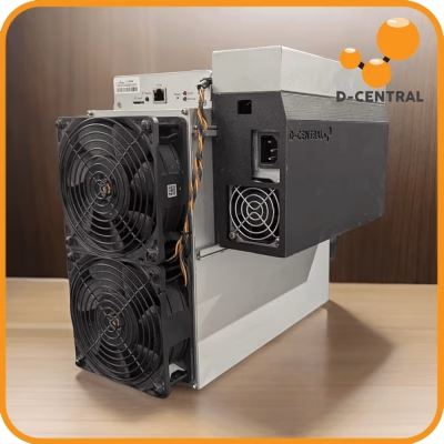
Individual ASIC dies are packaged in BGA (Ball Grid Array) or similar packages that provide electrical connections and thermal dissipation. These packaged chips are then soldered onto hashboards — the PCBs that live inside mining machines. A typical Antminer hashboard carries dozens of ASIC chips arranged in a daisy-chain configuration, with each chip contributing its hash power to the board’s total output.
If a chip fails or degrades, the entire hashboard can lose functionality. This is why professional ASIC repair requires both the diagnostic expertise to identify failed chips and the BGA rework skills to replace them — a service D-Central has provided since 2016 across 38+ miner models.
Why ASICs Matter for Bitcoin’s Security Model
ASIC mining is not just about efficiency and profitability. It is fundamental to Bitcoin’s security architecture.
Bitcoin’s proof-of-work consensus mechanism relies on the assumption that producing valid blocks requires real, physical, energy-consuming computation. ASICs make this computation as efficient as possible, which means more hashrate per dollar invested, which means a more secure network. The 800+ EH/s of SHA-256 hashrate protecting Bitcoin in 2026 represents an astronomical amount of physical infrastructure — millions of ASIC chips consuming gigawatts of power — and that infrastructure is what makes 51% attacks economically infeasible.
But there is a tension here that every serious Bitcoiner must grapple with: ASIC manufacturing is concentrated among a handful of companies, and large-scale mining operations tend to cluster around cheap power sources. This concentration risks undermining the decentralization that Bitcoin was designed to provide.
The Decentralization Imperative
This is precisely why home mining matters. Every hash computed outside of a data center is a hash contributing to network decentralization. Every miner running in a basement, a garage, or behind a hot water heater is a node of resistance against centralization.
The open-source mining movement — devices like the Bitaxe, NerdAxe, and NerdQAxe — represents a direct response to ASIC manufacturing concentration. These devices use commercially available ASIC chips (like the BM1366, BM1368, and BM1370) in open-source hardware designs that anyone can build, modify, and improve. They will not out-hash an Antminer, but that is not the point. The point is sovereignty. The point is that you, personally, are contributing hashrate to the network without asking permission from anyone.
At D-Central, we have been part of this movement since the beginning — we were the first company to manufacture the Bitaxe Mesh Stand, and we continue to develop heatsinks, cases, and accessories for open-source mining hardware. Decentralization of every layer of Bitcoin mining is not a slogan. It is our mission.
ASIC Chip Architecture: What Is Inside the Silicon
To truly understand mining ASICs, it helps to know what is happening at the chip level. While manufacturers guard their exact designs as trade secrets, the fundamental architecture of a SHA-256 mining ASIC is well understood.
Hashing Cores
The primary functional unit is the hashing core — a hardwired implementation of the SHA-256 compression function. Each core takes a block header candidate, runs it through 64 rounds of the SHA-256 algorithm (twice, since Bitcoin uses double-SHA-256), and outputs a hash. A modern mining ASIC contains hundreds to thousands of these cores operating in parallel.
Nonce Iteration Logic
Each hashing core systematically iterates through nonce values — the variable portion of the block header that miners modify to search for a valid hash. The chip manages the distribution of nonce ranges across its cores to avoid redundant computation.
Clock and Power Management
Mining ASICs operate at precisely controlled clock frequencies and voltages. Higher clock speeds produce more hashes per second but consume more power and generate more heat. The optimal operating point balances hashrate against energy efficiency and thermal limits. This is why overclocking and undervolting are common techniques among miners — and why understanding your ASIC’s thermal and electrical limits is critical for long-term reliability.
Communication Interface
ASICs on a hashboard communicate via a serial daisy-chain (typically SPI or a proprietary protocol). The control board distributes work (block header templates and nonce ranges) to each chip and collects results. When a chip finds a hash below the current target, it reports back immediately — that is a potential block solution.
The Economics of ASIC Mining in 2026
Mining economics come down to a simple equation: revenue from block rewards and fees minus the cost of electricity, hardware depreciation, and maintenance. ASICs are the central variable in this equation because their efficiency determines your electricity cost per bitcoin mined.
With the block reward at 3.125 BTC and network difficulty above 110 trillion, the margin between profitable and unprofitable mining is thinner than ever. At current difficulty levels, an Antminer S9 (0.098 J/GH) needs electricity below roughly $0.03/kWh to break even on mining revenue alone. An S21 (17.5 J/TH) remains profitable at electricity costs several times higher because it produces far more hashrate per watt.
But profitability is not the only calculation that matters. Home miners running older-generation ASICs as space heaters are not paying for electricity twice — the heat they produce offsets heating costs they would incur anyway. This dual-purpose mining model changes the economics entirely and extends the useful life of older ASIC generations far beyond what pure mining profitability calculations would suggest.
Maintaining and Repairing ASIC Hardware
ASIC miners are industrial hardware running at extreme power densities and temperatures. They require maintenance, and they eventually fail. Understanding the common failure modes helps you operate your equipment more effectively and know when to seek professional help.
Common ASIC Chip Failure Modes
Thermal degradation: Sustained operation at high temperatures degrades the semiconductor junctions over time. Chips may become less efficient, produce errors, or fail entirely. Proper cooling and airflow management are the first line of defense.
Electromigration: At nanometer-scale process nodes, the current density through metal interconnects can physically move atoms over time, eventually causing open circuits or shorts. This is a fundamental physics limitation that affects all semiconductor devices operating at high current densities.
Solder joint failure: The BGA solder balls connecting ASIC packages to hashboards can crack or develop cold joints due to thermal cycling. This is one of the most common repair scenarios — the chip itself may be fine, but its physical connection to the board has degraded.
Voltage regulator failure: The VRM (Voltage Regulator Module) circuits that supply power to ASIC chips can fail, causing the chips to operate outside their specified voltage range. This can manifest as reduced hashrate, increased error rates, or complete board failure.
D-Central’s ASIC repair service handles all of these failure modes across 38+ miner models from Bitmain, MicroBT, Innosilicon, Canaan, and more. With retail-focused repair since 2016, we have the diagnostic tools and BGA rework capabilities to get your hardware back to full hashrate.
The Future of Bitcoin Mining ASICs
The trajectory of ASIC development is constrained by semiconductor physics. We are approaching the practical limits of process node shrinks — 3nm is available today, 2nm is in development, but the gains in efficiency per node shrink are diminishing. The easy improvements have been made. Future gains will come from architectural innovation, better packaging, improved power delivery, and potentially new approaches like immersion cooling that allow chips to operate at higher frequencies without thermal throttling.
What This Means for Home Miners
As cutting-edge ASICs become more efficient but also more expensive, the home mining space benefits in two ways. First, older-generation hardware becomes available at steep discounts, making it accessible for dual-purpose mining (heating + hashing). Second, the open-source mining movement continues to mature, with projects like the Bitaxe putting current-generation ASIC chips into hardware designs that individual miners can own, operate, and modify without depending on any manufacturer.
The future of Bitcoin mining is not just bigger data centers with newer ASICs. It is also a distributed network of home miners, solo miners, and pleb miners running everything from repurposed S9s to open-source Bitaxes — all contributing hashrate to the most secure monetary network ever created. Every hash counts.
Frequently Asked Questions
What is an ASIC chip and why is it used for Bitcoin mining?
An ASIC (Application-Specific Integrated Circuit) is a chip designed to perform a single task — in Bitcoin mining, that task is computing SHA-256 hashes. Because the chip’s entire silicon area is dedicated to this one function with no wasted transistors on general-purpose logic, ASICs achieve hash rates and energy efficiency that CPUs, GPUs, and FPGAs cannot match. A modern ASIC miner produces over 200 TH/s while consuming around 17.5 joules per terahash.
How did Bitcoin mining evolve from CPUs to ASICs?
Bitcoin mining progressed through four hardware generations: CPUs (2009-2011), GPUs (2011-2013), FPGAs (2012-2013), and ASICs (2013-present). Each transition delivered orders-of-magnitude improvements in hash rate and energy efficiency. The first ASICs used 130nm process nodes; today’s leading chips use 5nm and 3nm processes, representing over 50x improvement in efficiency from the first ASIC generation alone.
Can you still mine Bitcoin without an ASIC?
Technically yes, but practically no — not if you expect to find blocks. With network hashrate above 800 EH/s and difficulty above 110 trillion in 2026, the probability of a CPU or GPU finding a valid block is vanishingly small. However, solo mining with small ASIC devices like the Bitaxe gives home miners a real (if small) chance at a full 3.125 BTC block reward while contributing to network decentralization.
What makes some ASIC miners more efficient than others?
Efficiency differences come from three main factors: the semiconductor process node (smaller nodes like 5nm allow more transistors in less space with lower power), the chip architecture (how the SHA-256 cores are designed and interconnected), and the power delivery and thermal design of the overall mining unit. A 5nm chip is inherently more efficient than a 16nm chip performing the same computation.
How long do ASIC mining chips last?
Under proper operating conditions — adequate cooling, clean power, and controlled environment — ASIC chips can operate for 5-10+ years. The primary enemies of chip longevity are sustained high temperatures, power surges, dust accumulation restricting airflow, and thermal cycling that stresses solder joints. Regular maintenance and proper ventilation significantly extend hardware life. When chips do fail, professional ASIC repair services can often replace individual chips rather than scrapping entire hashboards.
What is the difference between a mining ASIC chip and an ASIC miner?
The ASIC chip is the individual silicon die — the semiconductor component that computes hashes. An ASIC miner is the complete machine: hashboards populated with dozens of ASIC chips, a control board running the mining firmware, power supply units, fans, and a chassis. When people say “ASIC miner,” they mean the whole unit. When engineers say “ASIC chip,” they mean the specific integrated circuit on the hashboard.
Why does home mining with ASICs matter for Bitcoin?
Bitcoin’s security and censorship resistance depend on hashrate being distributed across many independent operators. When mining concentrates in a few large facilities, it creates single points of failure and potential vectors for regulatory capture. Every home miner running an ASIC — whether it is a full-scale Antminer repurposed as a space heater or an open-source Bitaxe solo mining on the kitchen counter — adds a node of decentralization to the network. This is not just hobbyist enthusiasm. It is critical infrastructure for Bitcoin’s long-term resilience.
Where can I get ASIC miners and replacement chips in Canada?
D-Central Technologies, based in Laval, Quebec, stocks a full range of ASIC miners, open-source mining devices, replacement ASIC chips, hashboards, and accessories. We ship across Canada and worldwide from our online shop. For miners that need repair, our ASIC repair service covers every major ASIC platform with diagnostics, chip-level BGA rework, and full hashboard restoration.