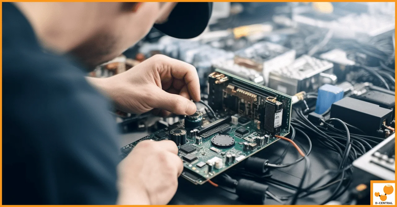
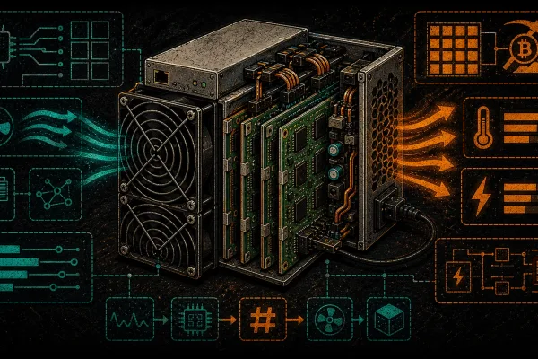
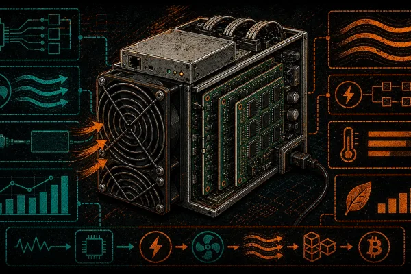
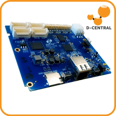
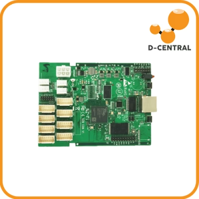
Open up any S9-through-S19-era Antminer control board and the biggest chip on it isn’t just a CPU — it’s a Xilinx Zynq, a hybrid part that pairs two ARM Cortex-A9 cores with an FPGA fabric on the same die. Most miners never think about that FPGA. But it is the reason the miner can feed work to hundreds of ASIC chips at hardware speed, and it explains several repair mysteries: why some faults survive a firmware reflash, why certain registers matter, and why newer boards work completely differently.
This is a plain-language tour of the data path between the control board and the hashboards, based on our bench work and on the open-source projects that documented this architecture — chiefly braiins/zynq-io (Braiins’ open FPGA design) and polprog/antminer_zynq.
The division of labour: CPU decides, FPGA transmits
On a Zynq control board the CPU never talks to the hash chips directly. The flow looks like this:
CPU → AXI bus → FPGA work/command FIFOs → UART TX/RX → hashboard chip chain
The mining software (bmminer/cgminer) prepares work and writes it over the AXI bus into FIFOs implemented inside the FPGA fabric. The FPGA then clocks that work out over UART lines — through level shifters, on pins 11 and 12 of each 18-pin data cable — to the daisy-chained ASIC chips on each hashboard. Responses (nonces) come back the same way. The FPGA’s register space sits at base address 0x43C00000.
The FPGA does more than shovel work. It also generates the VID signal used for voltage control, drives the fan PWM outputs, handles GPIO and the I2C buses shared with the hashboards, and runs CRC engines so data integrity checks don’t burn CPU cycles.
The two kernel modules that bridge the gap
Linux userspace reaches the FPGA through two small kernel modules loaded at boot by /etc/init.d/S10modules:
- bitmain_axi.ko creates
/dev/axi_fpga_dev, mapping the FPGA’s control and status registers so the mining daemon can poke them from userspace. - fpga_mem_driver.ko creates
/dev/fpga_memand allocates a 16 MB DMA buffer for work and nonce data (at memory offset 0x0F000000 on 256 MB systems).
If those modules fail to load, the miner boots, the web interface answers — and hashrate sits at zero, because the software has no path to the FPGA. It’s one of the failure signatures worth knowing when you’re reading kernel logs.
Why you can’t replace the bitstream
The FPGA’s configuration — the bitstream file soc_system.rbf — loads during early boot from BOOT.bin and is RSA-verified against keys burned into the SoC’s eFuses. On locked boards you cannot substitute your own FPGA design; the verification chain we mapped in our NAND boot-chain guide protects it end to end. Third-party firmware lives with the stock bitstream and replaces the parts of the system that are only SHA256-checked.
One historical footnote worth crediting: Braiins published their Zynq FPGA design as open source. Their generic dev-board design used SPI, while the S9 mining design uses UART IP cores — a detail that matters if you ever read that codebase expecting a 1:1 match with production boards.
The proof it can be done in software: BBB and Amlogic
Here’s the interesting twist for anyone who assumes the FPGA is irreplaceable: Bitmain itself shipped control boards without one. The BeagleBone-based boards (TI AM335x, late-2021 S19j/S19j Pro) and the Amlogic A113D boards (recent S19 family, S19 XP, S21, T21) drive the hashboards with software UART — no FPGA at all. On the Amlogic boards, each hashboard gets its own serial device (/dev/ttyS1 through /dev/ttyS3) with dedicated reset and detect GPIOs, the PSU sits on I2C at address 0x10, and fans hang off two PWM channels — all documented in skot/amlogic-cb-tools.
The trade-off is straightforward: simpler hardware and firmware, but the CPU carries the communication workload the FPGA used to absorb. Knowing which architecture you’re holding is diagnostic step one — our control board reference covers identification, and the Amlogic lock story explains why the newest boards add a firmware-lock wrinkle on top.
What this means at the repair bench
Three practical takeaways. First, a board that boots cleanly but shows zero hashrate with healthy hashboards deserves a look at the FPGA path — kernel modules loaded? devices present? — before anyone starts reflowing chips. Second, faults in the FPGA fabric or its supporting rails are board-level repairs, not firmware problems; no image will flash them away. Third, on FPGA-less boards the same symptoms shift meaning: serial devices and GPIOs replace FIFOs and AXI registers as your first suspects.
If a control board has you stumped, that’s bench work we do every week — ASIC repair in Montreal, control boards included. And if you want to go deeper on the architecture, the open-source repos above are the map we all stand on.
Component-level references
This guide is part of a bench-grounded series on the individual components of an Antminer control board and hashboard:
- Antminer NAND & boot chain — the partition map, the boot verification chain, and per-family recovery when a miner won’t boot.
- Hashboard EEPROM reference — what the EEPROM stores by generation and why boards aren’t interchangeable.
- The hashboard PIC microcontroller — what it does, how it fails, and why S21 boards have none.
- ASIC control-board reference — identify which control board you’re holding.